High spatial resolution cathodoluminescence
A key benefit of the cathodoluminescence (CL) technique over other luminescence characterization techniques is the ability to acquire information with high spatial resolution. Under the right conditions, spatial resolution approaching 1 nm can be achieved, far in excess of other optical techniques.
However, in order for the cathodoluminescence technique to achieve such high spatial resolution information there is a variety of experimental, instrumental and sample related factors which may need to be optimized.
Electrons as an excitation source
Electron microscopy (EM) effectively bypasses the Abbé resolution limit of conventional far field optical microscopy techniques where the resolution is approximately limited to the wavelength of the light used. The electron beam of a scanning or transmission electron microscope can be focused to a sub-nanometer diameter and used as an excitation source for luminescence measurements. Furthermore, an electron probe is extremely flexible due to the ease of scanning, focusing, and the large depth of field. The high vacuum of conventional electron microscopes can also provide an ideal environment for cryogenic cooling of specimens.
Spatial resolution of an electron microscope
For electron microscopes the spatial resolution in standard scanned-imaging modes is largely determined by the diameter of the focused electron beam which is rastered across the specimen. The incident spot size is determined by the spatial and energy profile of the electrons emitted by the electron gun, the quality of the column electron optics and the working distance. Remarkable progress has recently been made in field emission gun and column performance in terms of reducing spot sizes whilst providing high incident beam currents with beams focused to only a few angstrom (Å).
The generation volume (bulk material)
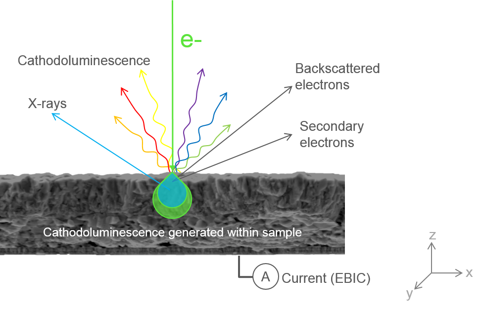
In a modern scanning electron microscope (SEM), the diameter of the focused electron beam (and hence SE image resolution) can be optimized to be a weak function of the accelerating voltage used within the electron column. However, for imaging or mapping using CL or x-rays, the spatial resolution is strongly influenced by the interaction of the landing electrons and the specimen: a high energy electron penetrates the sample transferring energy through a series of inelastic scattering events. In turn, the sample can release this energy through the emission of a CL or x-ray photon; many photons can be emitted as an electron loses all of its initial energy. The region from which CL (or x-ray) photons are emitted is usually termed the generation volume and can be modeled using Monte-Carlo simulations. In a slight oversimplification the generation volume scales laterally and vertically with the initial electron energy to the power 1.7 and is somewhat larger for CL than for x-ray photons because of the smaller energy needed to generate a CL photon, Figure 1.

High spatial resolution cathodoluminescence in bulk specimens (CL in SEM mode)
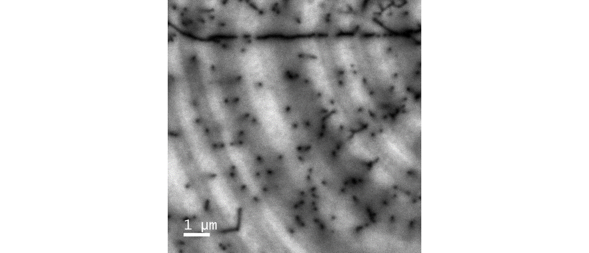
For most bulk specimens the simplest criterion for obtaining high spatial resolution CL is to use conditions where the generation volume will be small e.g., low primary electron energies (accelerating voltage), see Figure 2 for example. However this has some important consequences:
- Lower signal levels—lower electron energies means that less energy is transferred to the specimen (in semiconductors this represents fewer electron hole pairs) resulting in fewer CL photons being created.
- Introduction of surface effects—the region of the sample interrogated is closer to the surface as the vertical dimension of the generation volume is smaller. The surface region is where non-radiative recombination can dominate, e.g., where the CL is effectively killed. This surface “dead layer” can be due to polishing damage, surface recombination or surface electric fields that separate electron hole pairs.
- A higher injection density—a smaller generation volume necessarily dictates a higher carrier concentration as the same flux is injected into a much smaller volume. A higher injection density usually means lower CL emission (due to saturation effects) and is usually undesirable due to: local non-equilibrium conditions, unwanted beam induced changes to the specimen, luminescence saturation and quenching effects, and in extreme conditions on cryogenic specimens, heating effects. Hence optimum conditions for high spatial resolution CL often involve both low kV and low beam currents.
Hence, for CL experiments, the most sensitive apparatus should be employed for optimum results.

Cathodoluminescence in thin specimens (CL in STEM mode)
In a thin specimen the effect of the generation volume on spatial resolution is considered to be negligible and a spatial resolution approaching the diameter of the focused spot can be achievable—this is the principle behind using a scanning TEM to obtain very high spatial resolution CL.
Thin is a relative term and will depend on the sample under investigation and the energy of the electron beam but is typically a sample thickness <250 nm and <100 nm in a STEM and SEM instrument respectively. However, the light levels are necessarily low for several reasons:
- In a thin sample little energy is transferred from the electron beam to the sample which means that the CL signal will be low. With a semiconductor sample in the TEM it has been demonstrated that there is a tenfold increase in CL emission on reducing the accelerating voltage from 200 – 100 kV.
- The relatively proximity of the surfaces mean that non-radiative processes can be much more significant than in bulk materials acting to kill radiative recombination in semiconductor samples if the specimen is too thin.
Luminescence signals are highly sensitive to the presence of non-radiative recombination sites e.g., point defects in semiconductors. The high energy electron beams used in the TEM typically generate small numbers of point defects via a knock-on damage mechanism efficiently quenching the CL signal. Use of a low accelerating voltage, cryogenic temperatures and efficient detection can minimize beam induced effects.
Highly efficient collection and detection of CL is imperative from thin samples.
Specimen considerations
Specimen types
Insulators: minerals, ceramics, etc.
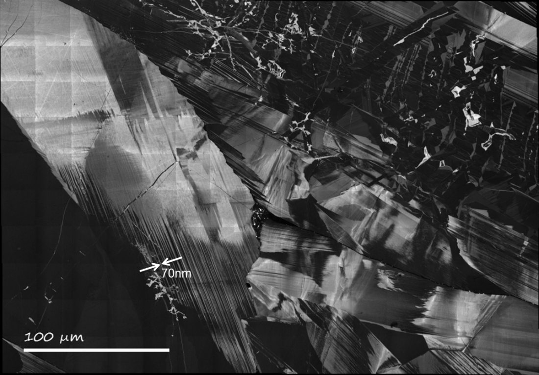
For geological specimens the spatial resolution is determined by the size of the generation volume under the minimum accelerating voltage that is practically useable. Due to the reduction in CL intensity under these conditions and the impact of surface dead layers careful sample preparation is required; the standard polishing techniques for optical microscopy, which do not eliminate fine scale surface abrasions, may limit conditions to greater than 10 kV. However, more careful polishing techniques to give a mirror finish can be employed which allow lower kV results giving spatial resolution better than 100 nm, Figure 3.
It should be noted that the spatial resolution of CL in a flood gun set up (rather than a focused probe) is still limited by the Abbé diffraction limit.

Semiconductor samples
In a bulk specimen, high resolution CL results cannot be achieved if the region of interest is buried relatively deeply. The primary concern is that the region of interest in the specimen (taking into account any surface dead layer) has to be accessible by the generation volume e.g., at, or very close to, the surface. In some cases this may mean special consideration is needed when preparing a sample e.g., by interrupting the growth of LED or laser diode structures.
An alternative approach for semiconductor specimens is to perform measurements in cross section. Although this can give the best high spatial resolution results, this approach is invariably destructive and necessarily probes a much smaller area of material for analysis. In this mode measurements at low accelerating voltage and low beam currents have demonstrated spatial resolution better than 20 nm.
In semiconductor samples, the luminescence does not necessarily originate from where an electron-hole pair was created: electrons and holes created by the electron beam are free to move within the sample (via drift or diffusion mechanism) before they recombine, thus, the CL photon can be emitted from a location remote from the generation volume. One consequence of this is that the spatial resolution is not defined easily a priori as the local minority carrier diffusion length is usually not well known and the spatial resolution will be a convolution of the generation volume size and movement of carriers before recombination. In samples with low minority carrier diffusion lengths (such as nitride semiconductors) the spatial resolution in bulk-like specimens can still be better than 50 nm. Although this apparent reduction in spatial resolution could be considered a downside it also enables CL to be a highly useful tool in studying the movement of free carriers.
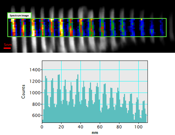
Many specimens and devices of interest are not simple bulk-like structures but are structured in some way either e.g., morphology or heterostructures making quantum wells. Often, the impact of this is that free carrier movement is restricted due to the introduction of potential barriers and the spatial resolution of a CL image or map appears to be higher. Researchers have taken advantage of this by demonstrating 20 and 2 nm quantum well/barrier structures to be resolved in the SEM and TEM respectively, Figure 4.

Plasmonics
The luminescence mechanism from metallic structures differs from semiconductor and insulator materials as there is no recombination of an electron and hole across a forbidden energy gap. Instead the luminescence results from the radiative decay of a surface plasmon. When a metal is exposed to a high energy electron beam bulk- and surface-plasmons are generated (oscillations in the sea of free electrons associated with interaction with a moving charged particle). Only luminescence generated close to the surface of the material escapes because of the efficient re-absorption processes.
The spatial resolution is effectively limited by the propagation of surface plasmon waves and the skin depth of the material. In practical cases, the best spatial resolution is typically (a few) tens of nanometers.
Topography
Luminescent specimens which show surface structure, whether in the form of growth structures, etch pits or porous etching structures, asperities, or device structures will often show enhanced spatial resolution. This is because generation, which also includes differences in back scattered electrons, will be influenced by the topography.
Cryogenic CL
The use of cryogenic temperatures can be highly beneficial for CL studies, often increasing the CL signal intensity and reducing the sensitivity of the specimen to electron beam damage—this is particularly useful when using the high electron energies associated with a TEM.
Cryogenic temperatures often enhance the CL emission very significantly. The size of the effect depends on the physics of the luminescence. For luminescence associated with rare earth, an “extrinsic” impurity for example, in geological specimens, there is little or no effect. However for semiconductor specimens, the effect of cooling with liquid helium can be an increase in signal by several orders of magnitude.
The general explanation is that radiative recombination becomes more favorable as the temperature falls compared to competing non-radiative recombination events. In addition for reduced dimension materials, the quantum confinement becomes enhanced thus leading to significant differences in the radiative recombination probability.
Hence a large increase in CL at cryogenic temperatures can enable high spatial resolution simply due to the fact that a signal can be measured at the low injection conditions.
Conclusions
CL performed in an SEM or TEM offers optoelectronic characterization with a flexible probe which is not restricted by Abbé diffraction limits, or near field restrictions. The spatial resolution is determined principally by the size of the generation volume but is also influenced by specimen characteristics e.g., specimen configuration, diffusion lengths, emission and absorption characteristics, and surface effects; with an appropriate specimen, a spatial resolution better than 20 nm has been demonstrated in the SEM whereas better than 2 nm has been demonstrated in the TEM.
For best results, optimal collection and detection apparatus is equally important as specimen characteristic.