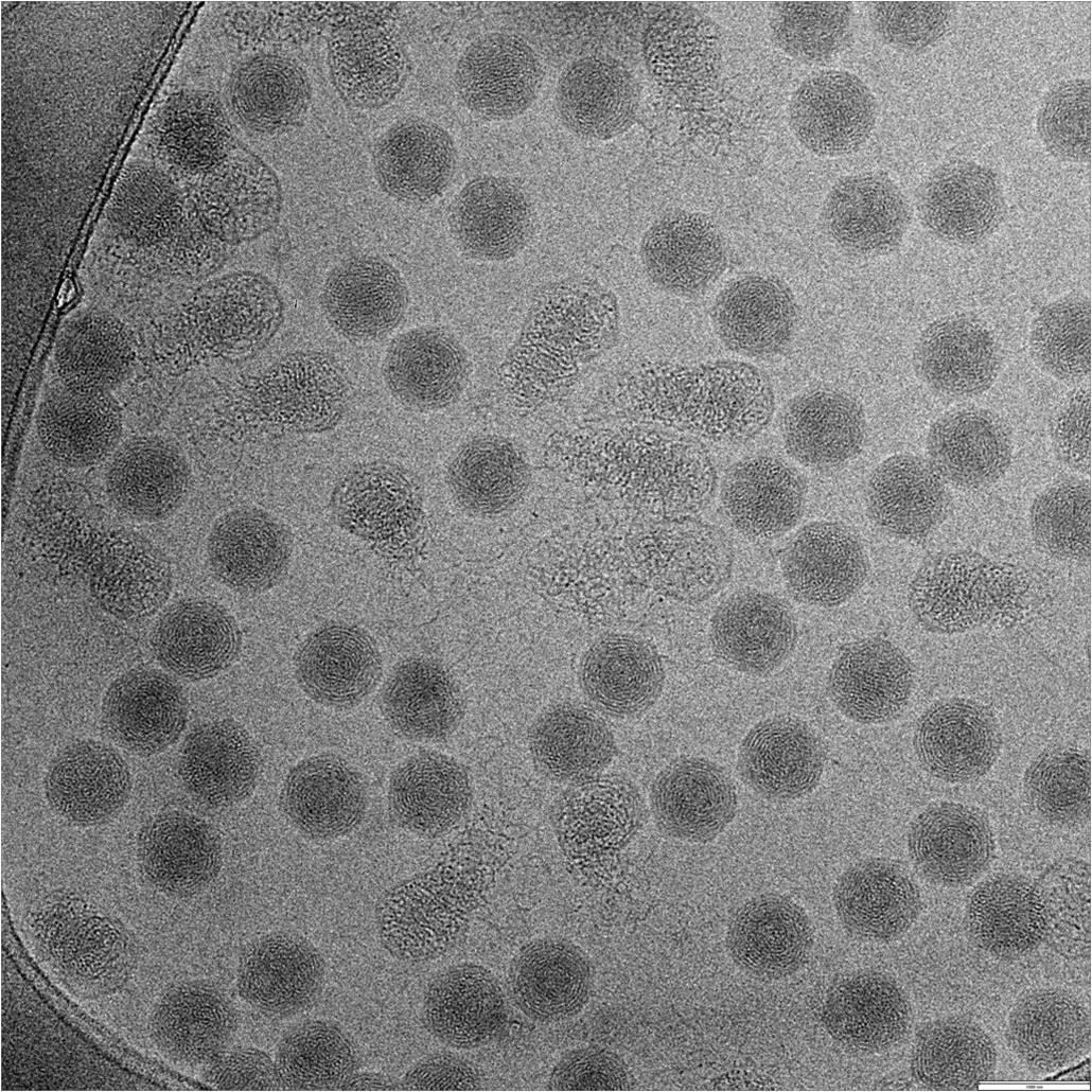
Cryo-EM images of T7 phage
Image courtesy of Dr. Zheng Liu, Markey Center for Structural Biology, Department of Biological Sciences, Purdue University
Grid was prepared using Cryoplunge™ 3 instrument. Image was recorded at 300 keV using 626 liquid nitrogen cryo-transfer holder.
Scale bar 100 nm
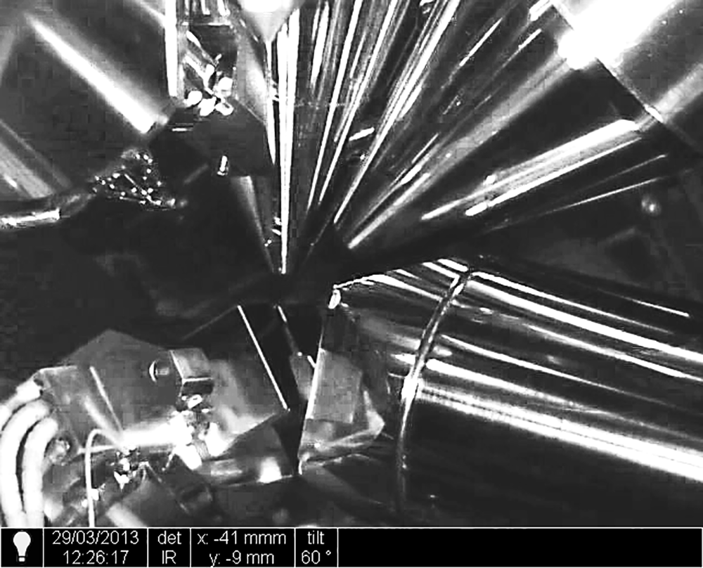
Murano heating stage for EBSD studies
Special compact design and heating method allows study of dynamic EBSD phase transformations within tight geometry restrictions of SEM.
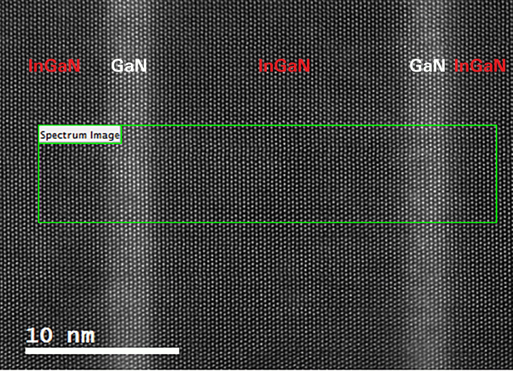
Atomic level EELS prepared in PIPS II system following FIB preparation (image 2)
Data courtesy of Dr. Phil Rice and Dr. Teya Topuria, IBM, San Jose, CA
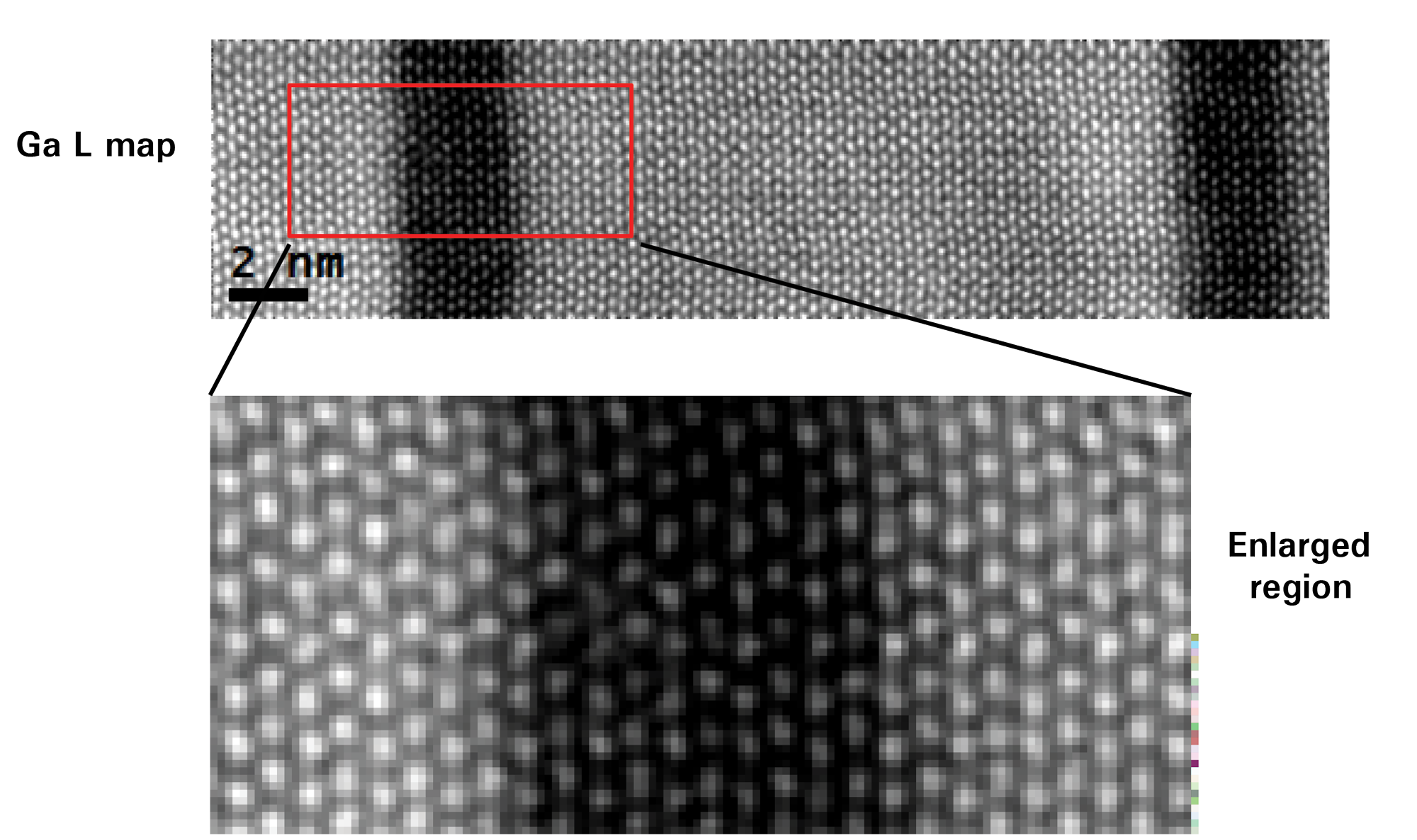
Fast atomic EELS analysis GaN/InGaN multi-layers sample preparation with PIPS II system and analysis with Gatan EELS product.
Atomic level EELS prepared in PIPS II system following FIB preparation
Data courtesy of Dr. Phil Rice and Dr. Teya Topuria, IBM, San Jose CA
Fast atomic EELS analysis GaN/InGaN multi-layers sample preparation with PIPS II system and analysis with Gatan EELS product.
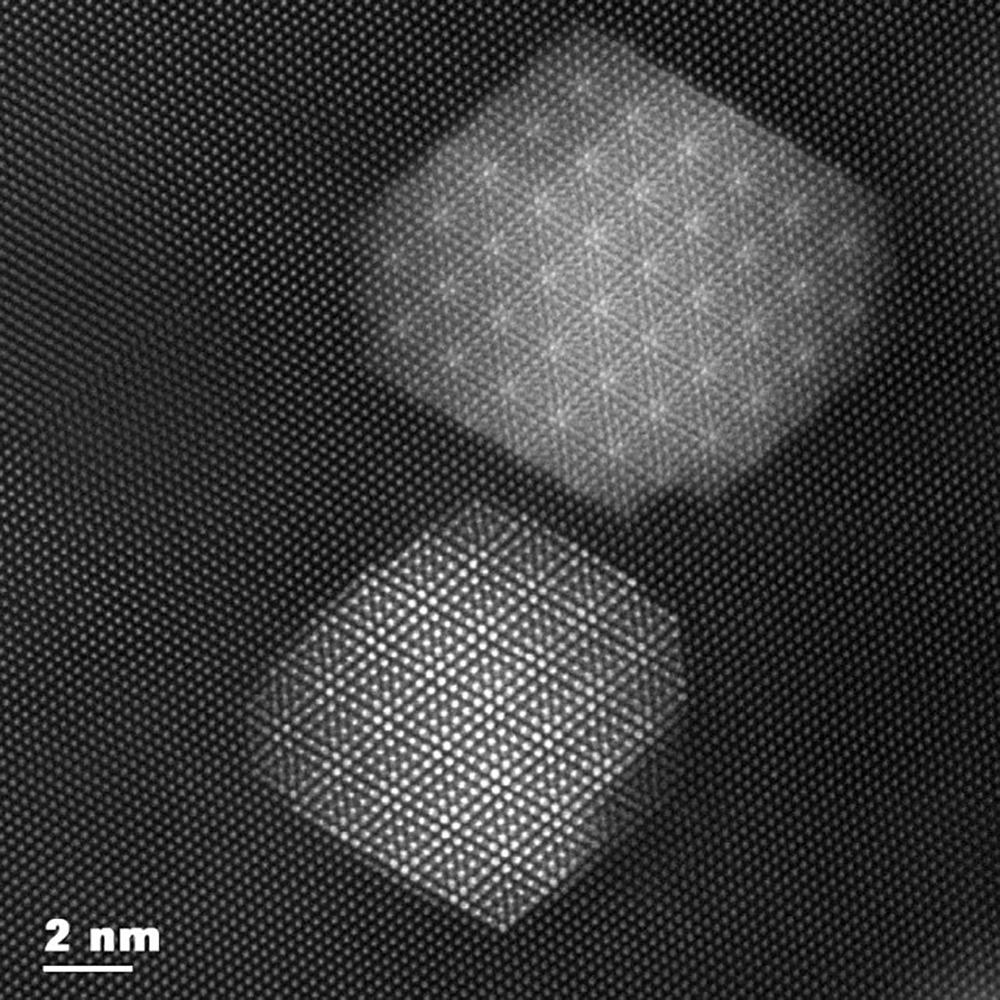
AlPb melt-spun ribbon with 1 - 3% at wt Ga HR-STEM using TEAM 0.5
Data courtesy of Anna Moros, Prof. Dr. Gerhard Wilde research group, Institute of Materials Physics, University of Muenster
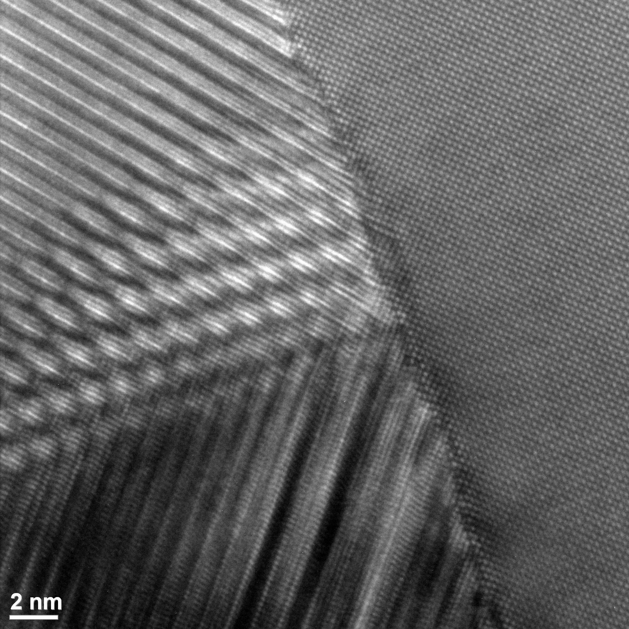
Ca3Co4O9 on SrTiO3 substrate
Data courtesy of Hanns-Ulrich Habermeier and Petar Yordanov, Max Planck Institute for Solid State Research, Stuttgart
TEM sample preparation and HRTEM image using a JEOL 4000FX TEM courtesy of Marion Kelsch and Peter A. van Aken, Stuttgart Center for Electron Microscopy, Max Planck Institute for Intelligent Systems, Stuttgart
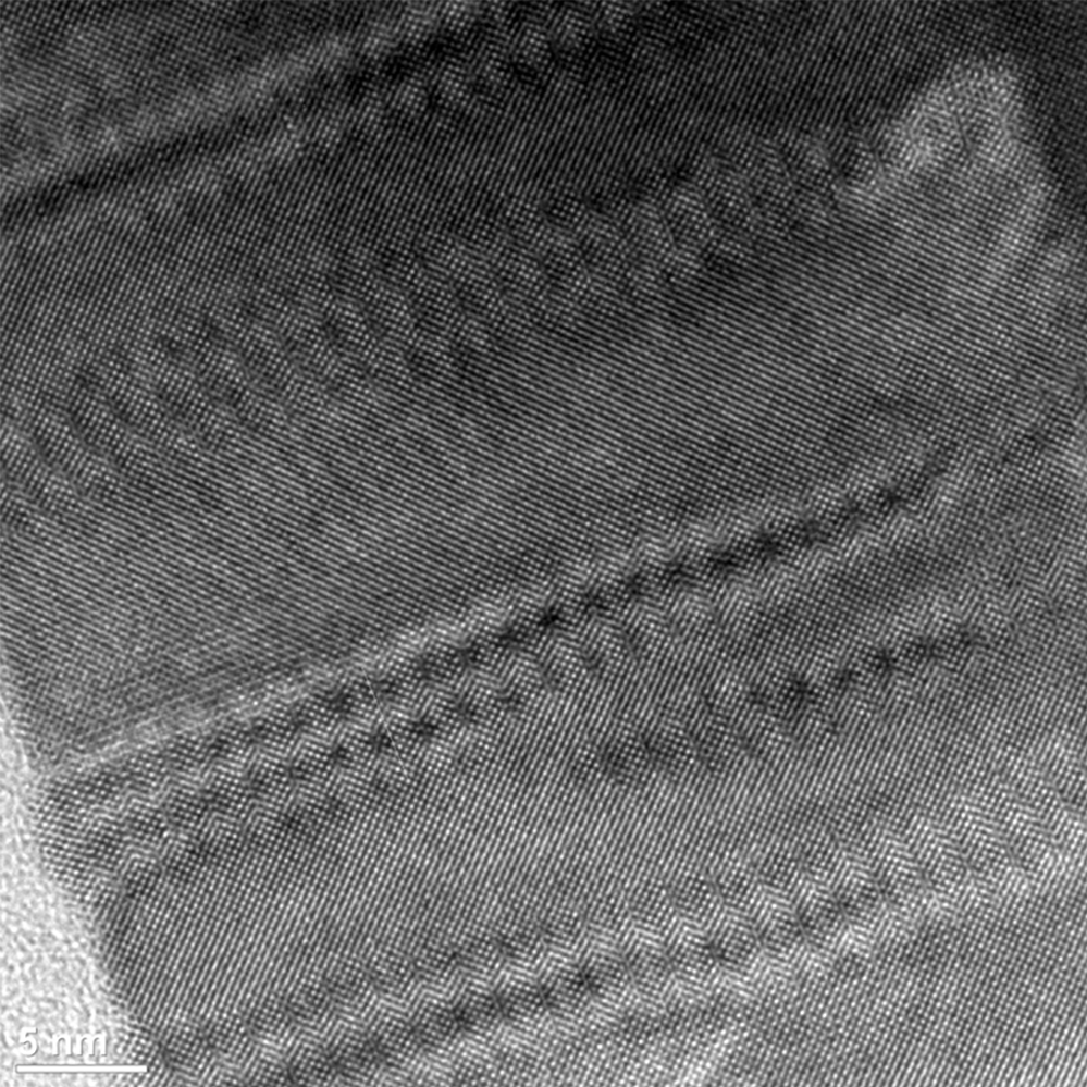
Sample La23Sr13MnO3 + 30% ZrO2 on LaAlO3 substrate
Data courtesy of Hanns-Ulrich Habermeier and Yuze Gao, Max Planck Institute for Solid State Research, Stuttgart
TEM sample preparation and HRTEM image using a JEOL 4000FX TEM courtesy of Marion Kelsch and Peter A. van Aken, Stuttgart Center for Electron Microscopy, Max Planck Institute for Intelligent Systems, Stuttgart
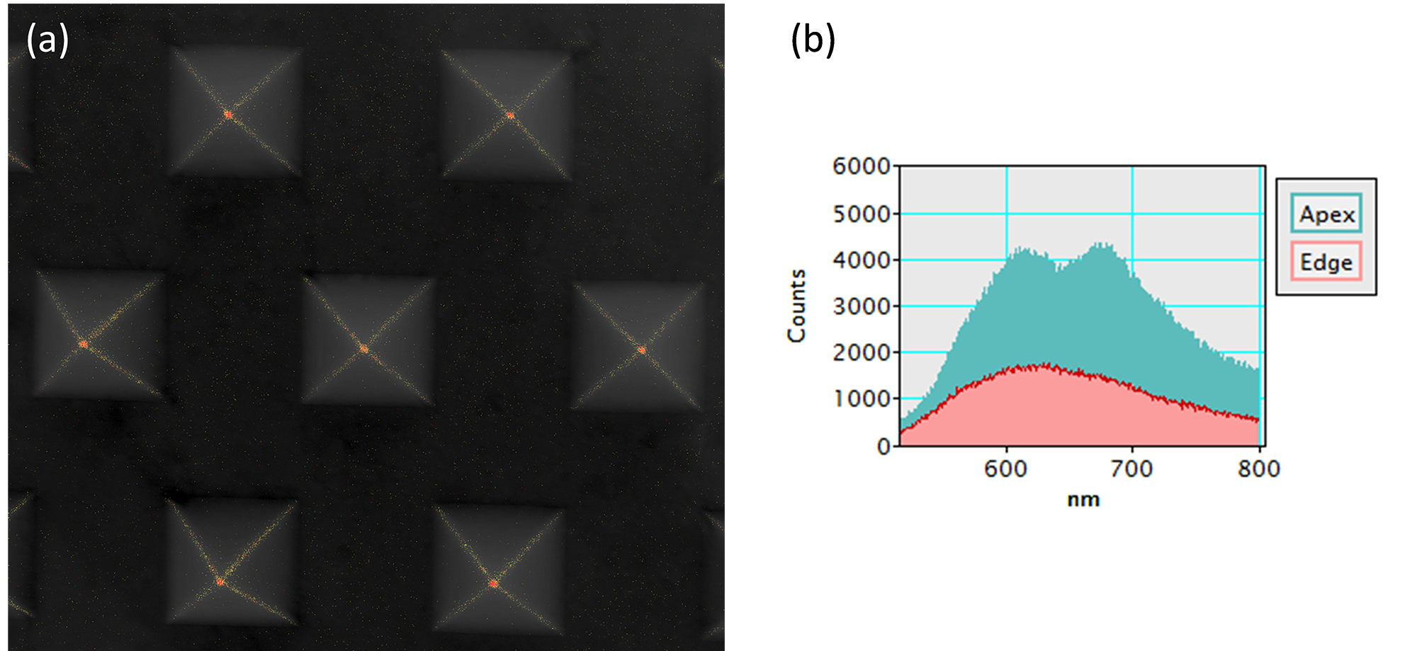
Surface plasmon resonance modes
Local surface plasmon resonance mode (LSPR) mapping of gold pyramids using cathodoluminescence. (a) Composite image of secondary electron image (gray) and, 650 nm (green) and 750 nm (red) monochromatic cathodoluminescence images. (b) Cathodoluminescence spectra from edge and apex of the pyramid in the center of image (a). LSPRs at apex and edges of pyramid are revealed to be 670 nm (1.85 eV) and 620 nm (2.0 eV) emissions, respectively. Acquisition time 2 s/spectrum.
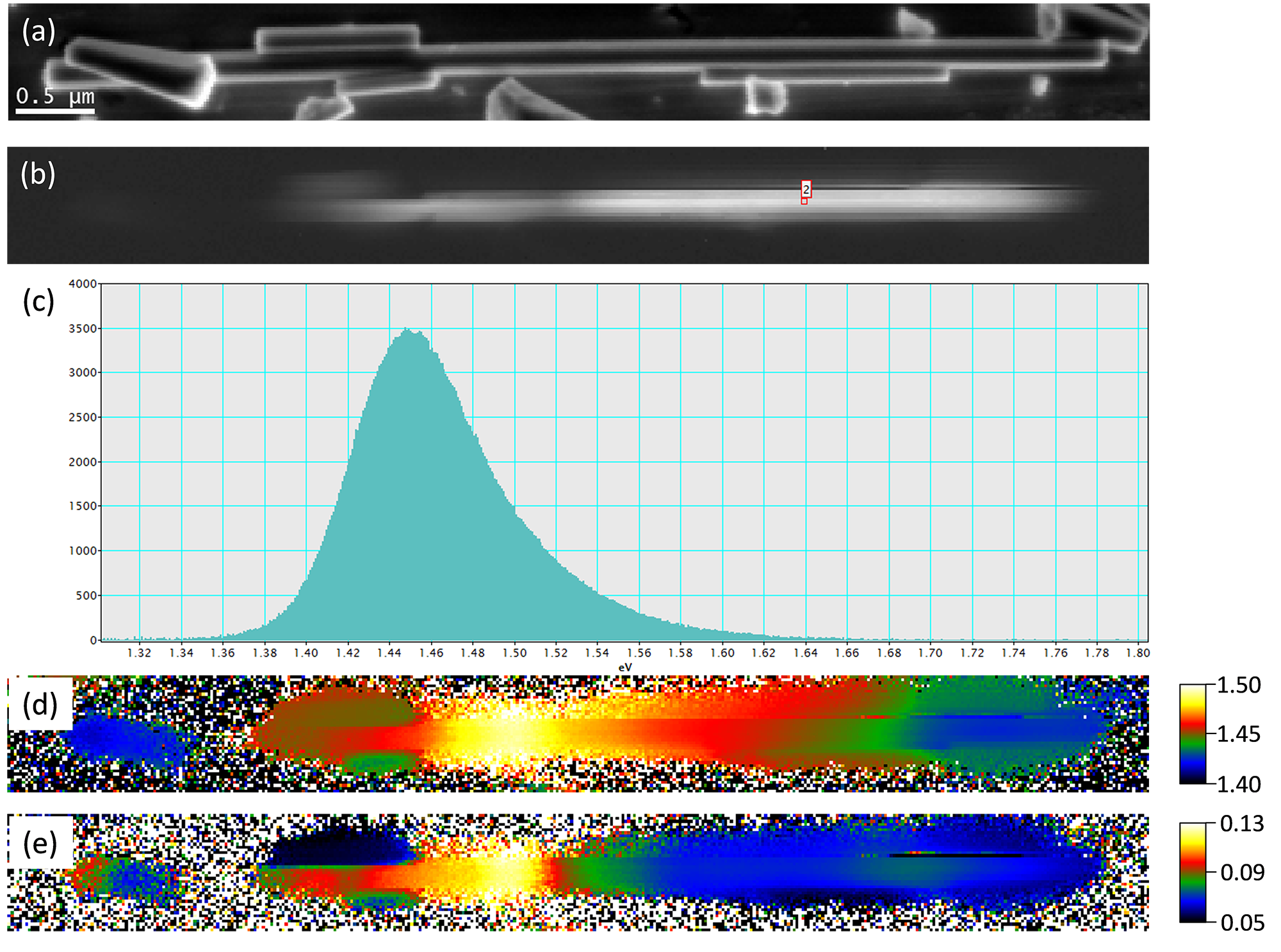
Cathodoluminescence spectrum-imaging of a gallium arsenide (GaAs) nanowire
Data courtesy of Dr. U. Jahn, Paul-Drude-Institut für Festkörperelektronik.
(a) Secondary electron image of a 200 nm diameter GaAs nanowire; (b) Cathodoluminescence spectrum-image displaying energy plane 1.46 ± 0.02 eV; (c) Individual cathodoluminescence spectrum extracted from spectrum-image with single peak at 1.45 eV; (d) Map of central energy of luminescence; change in wavelength is associated with a transition from zincblende (1.425 eV) to wurtzite crystal structure; wurtzite phase is calculated to have 55 meV larger band gap than zincblende phase; (e) Map of FWHM along nanowire.
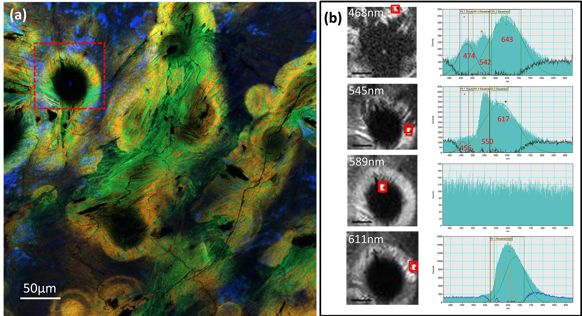
Cathodoluminescence spectrum imaging of polycrystalline diamond
Data courtesy of Dr. E. Vicenzi, Smithsonian Institute
(a) Composite cathodoluminescence image of polycrystalline diamond created using red, green, and blue spectrally filtered cathodoluminescence images. Radioactive fluid ingress along grain boundaries leads to radiation halo effects being observed (yellow).
Pages
