
NiAl-(Cr,Mo)共晶合金の相解析と微小方位差解析
はじめに
NiAl-(Cr,Mo) 共晶合金は、高融点、良好な耐酸化性、低密度を兼ね備えているため、高温での使用が期待されている材料である。本合金は、Cr,Moが固溶した体心立法う構造の不規則相により強化されたB2型規則構造の NiAl相により構成されている。結晶学的には、B2構造はNiとAlの2つの元素から構成されている体心立方構造である。この二つの結晶構造は原子位置が同じであるため、従来の電子後方散乱回折(EBSD)を用いた相判別方法では相分離を行うことが困難である
このアプリケーションノートでは、エネルギー分散型X線分光法(EDS)と組み合わせた透過EBSD法(TKD)を使用し、クリープ試験を行った共晶NiAl-(Cr,Mo)合金の相を観察した。Hough変換による指数付け(HI)、Spherical indexing(SI)と同時取り込みしたEDSとの組み合わせによるEDAX® ChI Scan™ でを行い、方位・方位差・相の解析を行った。
測定方法
試料の作製: NiAl-(Cr,Mo) 共晶合金をブリッジマン法で鋳造した。試料はクリープ試験後に測定された。
薄膜の加工:Ga⁺ 集束イオンビーム(FIB)によるミリングとリフトアウトにより電子透過性ラメラが調製された。
TKD–EDS データ収集:EDAX APEXソフトウェアで制御されたEDAX® Velocity™ EBSD検出器とEDAX Octane Elect EDS検出器を使用して、TKDとEDSデータを同時に収集した。7 x 6 µmの領域を10 nmのステップサイズにて、試料は水平に対して20°逆傾斜で観察を行った。
指数付けとデータプロセス: パターンは最初にHough変換による指数付けを行い、Spherical indexによって再指数付けされ、その後、ChI-ScanによるSpherical indexでリファインされ、EDSからの元素情報は、OIM Matrix™モジュールを備えたEDAX OIM Analysis™(v 9.1)ソフトウェアを使用して相の割り当てに組み込まれた。
結果と考察
方位マップ
HIによる逆局点図(IPF)マップには、特に結晶粒界近傍や変形領域で解析不良点が存在している。Spherical indexを行うことで、解析不良点が大きく減少し、粒界近傍でも安定して方位を決定することができている。(図1)
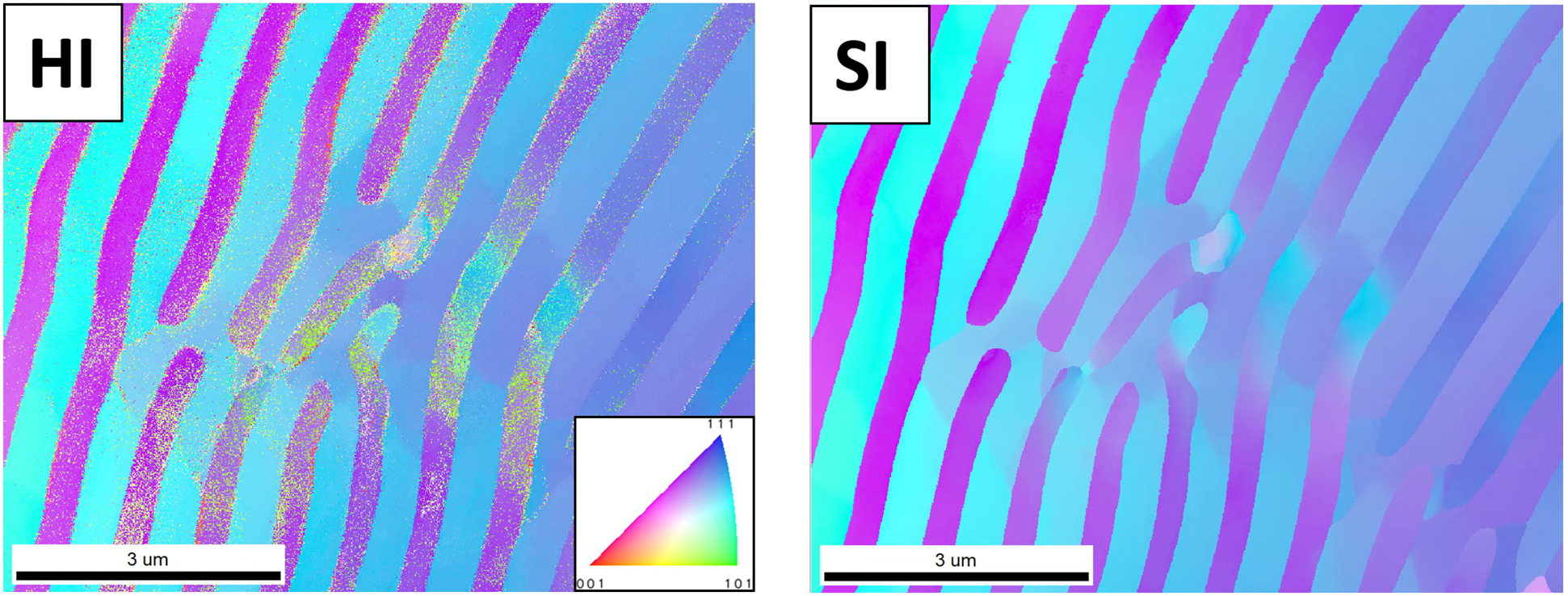
Figure 1. IPF ND orientation maps of the TKD dataset. Left) Initial Hough indexing shows scattered misindexed pixels at boundaries and in high strain regions. Right) Spherical indexing suppresses these artifacts and sharpens boundary definition.
サブグレイン組織
Hough変換により指数付けから得られたKernel average misorientation(KAM)マップ(図2)では、サブグレイン粒界の区別が困難であった。角度分解能の高いSpherical Indexを行うことで、Hough変換によるKAMマップの角度方位ノイズによって不明瞭であったわずかな方位差のサブグレイン粒界を明らかにした。
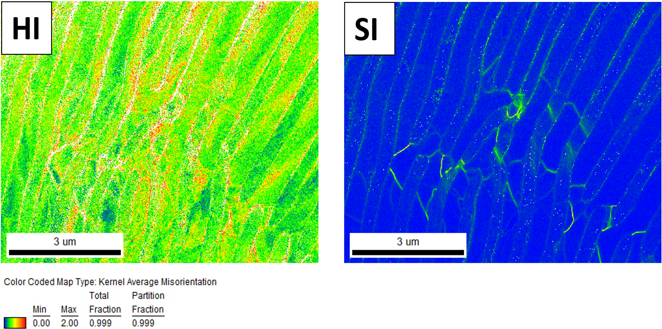
Figure 2. KAM maps (0 – 2°) created from HI (left) and SI (right). The improved orientation precision with SI resolves low angle subgrain boundaries that appear diffuse or fragmented in the HI based map.
EBSD単独の相マップ
B2型NiAlとbcc (Cr,Mo)は結晶学的に類似しているため、HIとSIの両方が相を確実に分離するのに苦労した。SIはHIよりも若干改善されたが、相の誤った割り当てが残った(図3)。B2とbccのシミュレーションマスターパターンは、バンド強度に微妙な違いがあるだけで、これらの条件で収集された実測の電子後方散乱パターン(EBSP)は、強い微細構造コントラストを示さない(図4)。このことは、純粋にパターンに基づくアプローチでは、この合金の相判別が困難であった理由を説明している。
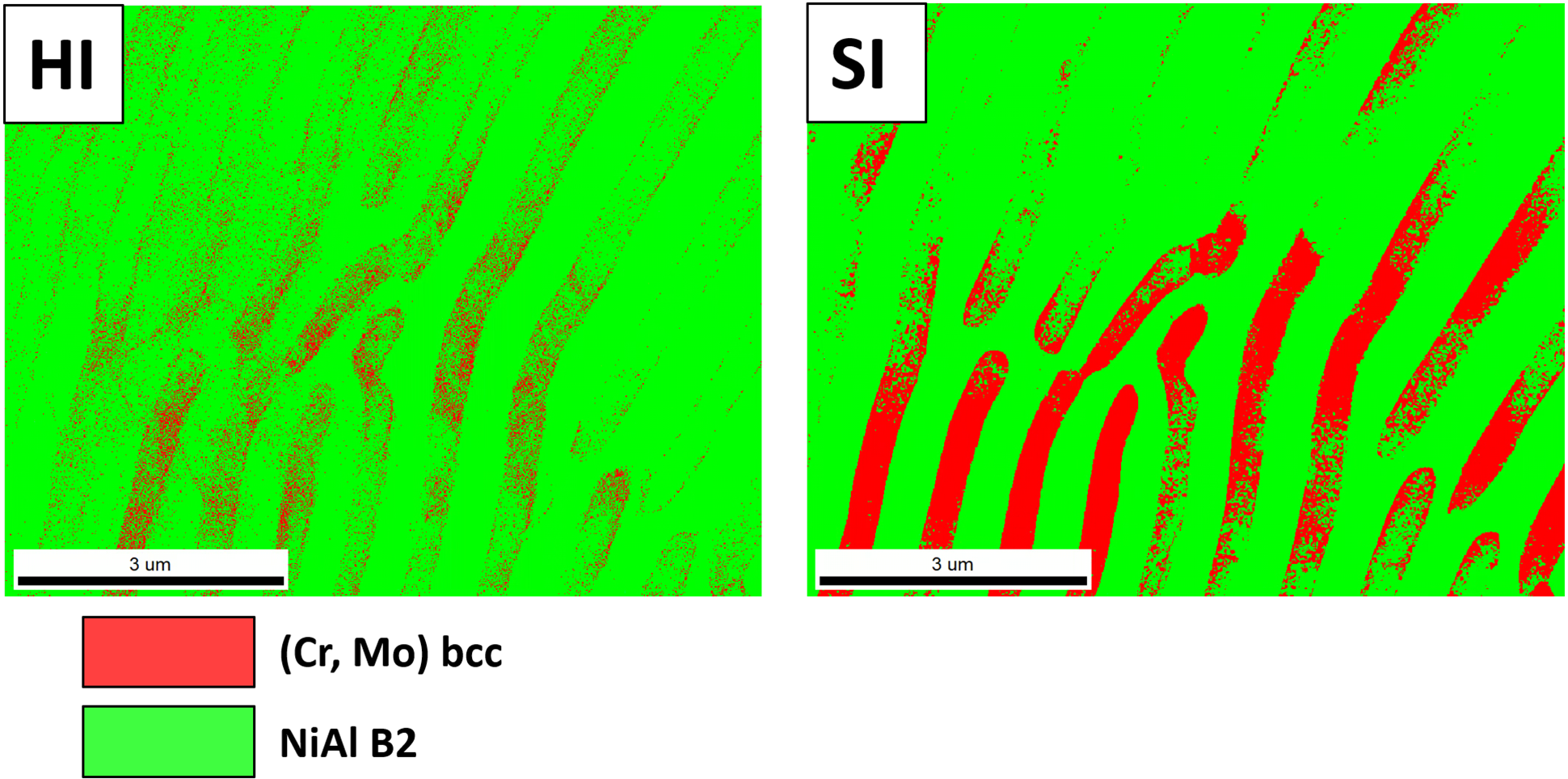
Figure 3. Phase maps produced with HI (left) and SI (right). Due to the crystallographic similarity of B2 NiAl and bcc (Cr,Mo), SI yields only a modest improvement and some misassignments persist.
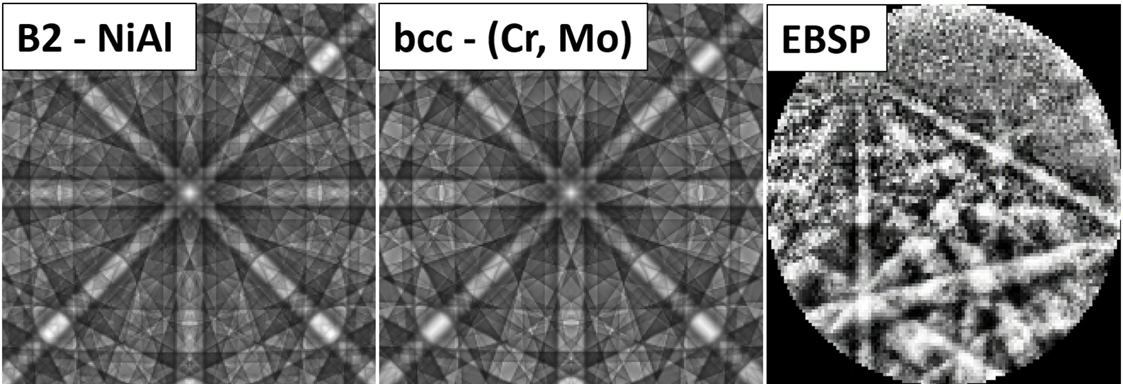
Figure 4. Simulated master patterns for B2 NiAl and bcc (Cr,Mo) exhibit only subtle band intensity differences; the representative experimental EBSP lacks the fine structure contrast needed for reliable phase discrimination.
EDSを使用した再指数付け (ChI-Scan)
同時取り込みで得られたNi Cr AlのEDS合成カラーマップにより、NiAlリッチ領域と(Cr,Mo)リッチ領域を明確に観察することができた。SIにChI-Scanを通してこの元素情報を組み込むことで、正しい相割り当てが可能になった(図5)。
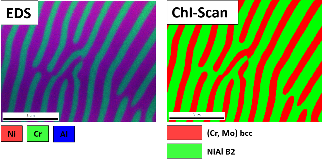
Figure 5. Blended EDS map (NiAl in purple; (Cr,Mo) in green) used during SI with ChI-Scan. Incorporating elemental context enables correct phase assignment in the final phase map while maintaining orientation quality.
まとめ
TKDによりNiAl-(Cr,Mo)共晶合金中のナノスケールのラメラを高い空間分解能で観察することに成功した。Spherical indexingは、Hough変換による指数付けと比較して、方位決定精度と方位差解析精度を向上させた。ChI-ScanはEDS信号を利用して、パターンだけの方法では区別できない結晶学的に類似した相を分離する。EDS/EBSD同時取り込み可能な構成とSpherical Indexの組み合わせにより、このようなナノスケール合金における相、方位、微小方位差のEBSD観察が可能になった。
謝辞
試料を提供頂いたDr. Steffen Neumeier (Institute for General Materials Properties, Friedrich Alexander Universität Erlangen Nürnberg)と特性評価や解析をして頂いた Dr. Johan Westraadt (Center for Electron Microscopy and Analysis, The Ohio State University) に感謝します。