About the NUANCE Center
The Northwestern University's Atomic and Nanoscale Characterization Experimental Center (...

The Northwestern University's Atomic and Nanoscale Characterization Experimental Center (...


The Northwestern University's Atomic and Nanoscale Characterization Experimental Center (NU...
The Northwestern University's Atomic and Nanoscale Characterization Experimental Center (NUANCE) was established by the founding director, Professor Vinayak Dravid during 2001-02. Guided by Professor Dravid’s vision, NUANCE integrates complementary analytical instruments and characterization capabilities at Northwestern University to address emerging opportunities for fabrication and characterization of soft, hard and hybrid materials, structures and devices. NUANCE serves Northwestern and the broader scientific and engineering community and provides invaluable resources to the private sector and public institutions in and around the Midwest. An operationally and fiscally efficient solution to the increasing need for advanced analytical and characterization instrumentation and fabrication tools, NUANCE leverages staff technical expertise to assist and collaborate with researchers in the physical sciences, engineering, and interdisciplinary fields.
For two decades, under the leadership of Professor Dravid, NUANCE has assisted thousands of award-winning faculty, scientists, engineers, medical doctors, and students with the facilities and skills required to carry out collaborative, interdisciplinary world-class nanoscale research. NUANCE actively seeks out partnerships with regional academic, governmental, and industrial agents. These collaborations are often geared towards the translation of nanoscience-based products, processes, and services to the market.
NUANCE mission is to provide and continually update state-of-the-art and core analytical characterization instrumentation and fabrication resources, with 24/7 open access, for the Northwestern community and beyond. The word “resource” includes not only mere “instrumentation and access,” but also hands-on training, education, research collaboration, and outreach. NUANCE aspires to be a pro-active and integral part of all scholarly activities related to characterization at Northwestern and beyond.
NUANCE provides core analytical characterization instrumentation resources in a collaborative environment, with 24/7 open-access for research and education, for the NU community and beyond. Within NUANCE, the EPIC was the first shared user facility that director Dravid conceived and formed in mid-1990’s to support a broad range of nanoscale science and technology projects, specializing in nanoscale analysis and characterization. EPIC is a multi-user, multi-departmental facility offering continually updated state-of-the-art equipment to qualified researchers from any field and institution. Managed by expert technical staff, EPIC instrument users have access to advanced electron microscopes and related sample preparation instruments. Highlighted amongst transmission electron microscope instruments are:
For more information about EPIC please visit their website.
Nanostructural features of new generation low-cost ultra-high-strength steels strengthened by dual phases of β-NiAl and M2C carbide
 Low and (b) high magnification bright field scanning TEM (BF-STEM) image showing the general microstructural features of aged AIR0509 steel. (c) [001]M electron diffraction pattern (EDPs) obtained from the circled region indicated in (a). (d) High resolution TEM (HRTEM) image along [001]M direction. (e) and (f) Fast fourier transform (FFT) patterns corresponding to region A and B indicated in (d). (g–l) Elemental maps corresponding to Al–K, Cr–K, Mo-L, Ni–K, Fe–K and Co–K respectively.")
Due to the high total detector area and large solid angle, the EDS capability of ARM 200CF is very effective in performing chemical analysis at high spatial resolution and with a high signal-to-noise ratio (SNR). The figure below illustrates the nanostructural analysis of a recently developed novel low-cost ultrahigh strength steel, which is hardened through a dual-phase strengthened mechanism. By conventional image analysis, we cannot observe the structural features of the precipitated phases. However, by means of high spatial resolution EDS analysis, we can clearly visualize the morphological features and the distribution of nanoscale precipitates. (1)
― Dr. Xiaobing Hu, TEM Facility Manager / Research Assistant Professor at NUANCE/MSE
Electron counting 4D STEM studies of electron beam-sensitive human tooth enamel
The Gatan K3 IS coupled with a STEMx system on our JEOL ARM300F were used to capture low-dose 4D STEM diffraction datasets (300 frames per second; dose ~200 e/Å) of human dental enamel, the outer layer component of human teeth. Understanding enamel structural details are of high importance in multiple human health contexts, from understanding enamel formation to the development of its defects. Enamel crystallites, the nanoscale building blocks of human enamel, can be investigated from the micro- to the atomic scale using (S)TEM, however, the sensitivity of this mineral to the electron beam is one of the limiting factors for performing such studies. Although recently atomic-resolution STEM imaging at cryogenic temperatures successfully revealed the apparent coherent atomic structure of crystallites in detail, (2) the field-of-view (FoV) was limited. While the 4D STEM dataset has a ~12x larger FoV, qualitative analysis of the difference in intensity between two opposing virtual segmented detectors reveals that certain individual crystallites display a tilt within the mineral lattice. This suggests that enamel crystallites may not be as coherent as previously thought, which in turn could have important implications on mechanical properties and provide unique insights in crystallite growth during enamel formation.
― Dr. Paul Smeets, Facility Manager FIB&TEM / Research Associate at NUANCE/EPIC
 Cryo-STEM image displaying part of an enamel crystallite (see ref. (2)) b) Average diffraction pattern of the 4D STEM data set (high SNR). Inset: single diffraction pattern of the 4D STEM data set (low SNR). c) Average diffraction pattern with 12 segmented virtual detectors (indicated by white lines). d) Virtual image created from the average diffraction pattern, combining intensities from all segmented virtual detectors. e,f) Maps displaying the differences in intensity between two selected opposite partial virtual detectors (indicated in inset). This difference in intensity is indicated in the red to blue color bar on the right. The black arrows indicate places within single grains that show variations in intensity between the opposed virtual detectors, which signify a tilt in the crystallographic directions of the apatite lattice with respect to one other. A special thanks to Dr. Roberto dos Reis & Stephanie M. Ribet for helping with data analysis using Python scripting.")
To view a full experiment brief click here.
Unconventional defects within quasi-one-dimensional KMn6Bi5 nanowires
. Spectrum imaging analysis of the plasmon peak variations among different domains (bottom left and right).")
Quasi-1D KMn6Bi5, which comprises ideal 1D nanowire (NW) motifs as an intrinsic part of the crystal structures and its defect mechanism is unusual in that the 1D nanowires slide linearly as a whole rather than conventional atomic displacements. Unconventional motific defects, which lead to two domains of inter-NW spacing larger or smaller than the pristine NW array, are unraveled by aberration-corrected scanning transmission electron microscopy (AC-STEM) images and corresponding multislice image simulation, which can image each atomic column using a sub-Å electron probe. (3) Inter-NW spacings without compositional or structural modulation can shift bulk plasmon energy at two different domains using electron energy loss spectroscopy (EELS) at the low energy range of 0-50 eV, which can measure optical and electronic properties such as the bandgap, local density of states (LDOS) and bulk/surface plasmon excitation.
1) Gao, Y. H., Liu, S. Z., Hu, X. B., Ren, Q. Q., Li, Y., Dravid, V. P., and Wang. C. X. (2019) A novel low cost 2000 MPa grade ultra-high strength steel with balanced strength and toughness. Materials Science and Engineering A, 759, 298-302. https://doi.org/10.1016/j.msea.2019.05.039
2) DeRocher, K. A., Smeets, P. J. M., Goodge, B. H. et al. Chemical gradients in human enamel crystallites. Nature 583, 66–71 (2020). https://doi.org/10.1038/s41586-020-2433-3
3) Jung, H. J., Bao, J. -K., Chung, D. Y., Kanatzidis, M. G., and Dravid, V. P. (2019) Unconventional Defects in a Quasi-One-Dimensional KMN6Bi5. Nano Letters 19(10), 7476-7486. https://doi.org/10.1021/acs.nanolett.9b03237

An Office of Science user facility jointly operated by Los Alamos and Sandia National Laboratories.
The Center for Integrated Nanotechnologies (CINT) offers world-leading scientific expertise and specialized...
An Office of Science user facility jointly operated by Los Alamos and Sandia National Laboratories.
The Center for Integrated Nanotechnologies (CINT) offers world-leading scientific expertise and specialized capabilities to create, characterize, and integrate nanostructured materials at a range of length scales, from nano- to meso-scale. CINT helps scientists perform cutting-edge research in the areas of nanoscience and nanotechnology, providing FREE ACCESS for nonproprietary research. CINT facilities are open to the international research community, including government, academic, and industry researchers.
One of CINT’s core research areas is in-situ S/TEM experiments. Early capabilities focused on electrical and electrochemical property measurements of materials during high-resolution imaging. More recently, the staff has expanded the available techniques to include gaseous environments (ETEM), liquid-cell, mechanics, ion irradiation, laser ablation, cryogenic, heating, and air-free transfer. In-situ investigations have focused on coupled structure-property measurements on real materials, with the CINT user community expanding many of the in-situ method developments.
Energy Storage: Solid-liquid interfacial reactions control the performance of many of today’s portable energy storage technologies. Understanding the mechanisms of ion transfer across these interfaces provides critical insight for engineering solutions to improve performance, such as artificial solid-electrolyte interphases. CINT can analyze these materials and systems using a variety of techniques.
Soft Matter and Beam Sensitive Materials: CINT recently established a cryo-TEM suite dedicated to minimizing the electron dose for imaging materials and interfaces in their native hydrated (or solvated state). This provides an optimized characterization of sensitive materials across multiple length scales. Instruments included are a Talos dedicated cryo-TEM, a Scios 2 Dual-Beam SEM/FIB equipped with a Leica cryogenically-cooled stage, and a Vitrobot for reproducible and controlled vitrification of hydrated samples. Uniquely, CINT also provides Leica cryogenic-transfer equipment including a sample-prep station (VCM), high-vacuum transfer shuttle (VCT500), and a cryogenically-cooled sputter coater (ACE600). This robust and complete workflow allows for the preparation of frozen, electron-transparent lamellae that can be transferred to the TEM without ever leaving a cryogenic environment.
Corrosion: Reactions at the surfaces of metals in contact with various solutions can cause massive structural deterioration, in the form of uniform, localized, and pitting corrosion. In-situ S/TEM has recently been proven as a method to investigate the initiation and propagation mechanisms of localized corrosion, with implications for progression mechanisms that cause pit formation.
Gas-solid Reactions: CINT offers a 300kV Titan G2 Environmental TEM which is monochromated, image-corrected, and equipped with a Gatan K2-IS camera. The gas cart provides high-level control over the inlet gas composition while minimizing contamination throughout the system. Many different studies may be conducted with an array of TEM holders. We also offer Protochips’ AXON software for minimizing image drift during in-situ reactions.

"Scientists should provide solutions to social problems and dreams for people."
The Nakamura Group is...
"Scientists should provide solutions to social problems and dreams for people."
The Nakamura Group is tackling this goal by means of physical organic chemistry and synthetic chemistry.
It has long been the dream of chemists to elucidate the intrinsic nature of atoms, molecules, and their assemblies, together with controlling their functions. We are exploring new concepts of structural chemistry and the creation of new functional materials using original synthetic tools developed by ourselves. We are also promoting research into the creation, property control, and biological function of molecular assemblies at angstrom or nanoscale level, and even above (nano-integration). This research is based on fundamental investigations into the structure and reactivity of organic molecules, using various tools such as high-resolution electron microscopy, scanning probe microscopy, and theoretical calculations, together with the development of powerful synthetic methods. These studies are supported by research grants from the Ministry of Education, Culture, Sports, Science, and Technology, with the ultimate goal to reach for scientific dreams, to sustain a healthy life, and to address environmental issues and resource depletion.
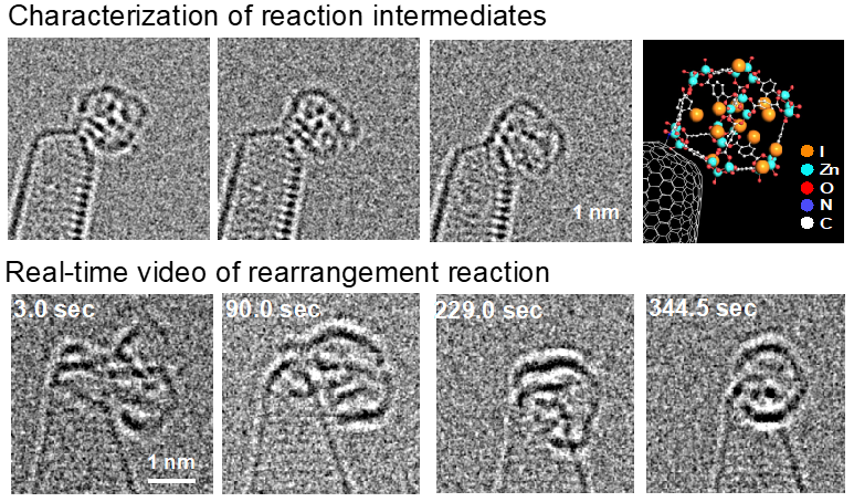
Real-time Video Imaging of Mechanical Motions of a Single Molecular Shuttle and Sub-millisecond Sub-angstrom Precision
Chemistry in motion: Researchers produce first-ever videos of chemical synthesis at atomic resolution
A scientists' dream: "Imaging single organic molecules in motion" is becoming a reality
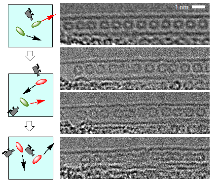
Since the concept of atoms and molecules was established a long time ago, it has been the dream of scientists to observe the motion of single small organic molecules. We showed in a 2007 Science paper1 that this is no longer a dream, by studying using a high-resolution electron microscope to in-situ record movies the motions of small organic molecules trapped in or attached to carbon nanotubes2. Since then, we reported movies of the conformational changes of a number of small molecules3 and even performed a kinetic analysis of chemical reactions by analyzing individual reaction events one by one by recording chemical events continuously by using a CMOS camera (Gatan OneView)4,5.
We can also study for the aggregation of single organic molecules leading to nucleation and crystal growth6. More recently, we have succeeded in isolating minute reaction intermediates at each stage in metal-organic framework synthesis and seeing how these changed with time7.
 Once considered too futuristic, this research is seeing rapid development owing to a state-of-the-art atomic resolution electron microscope in full operation in the basement of the Molecular Life Innovation building where our lab is located.
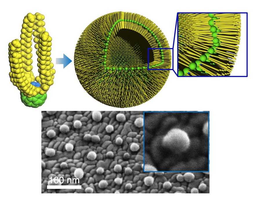
Functional carbon clusters: Synthesis, assembly, function, and applications
π-Conjugated organic compounds possess unique electronic properties and assemble to form functional materials. We have developed new carbon-rich p-conjugated materials (functional carbon clusters) and investigated their materials and biological applications. For example, when nanometer-sized [60]fullerene molecules are functionalized and aligned horizontally, water-tight fullerene bilayer membranes form and assemble into nanoscale vesicles8. We also achieved DNA and siRNA delivery to animals using an aminofullerene carrier9. In addition to these curved π-electron compounds, we have developed a rigid planar π-electron system, carbon-bridged oligo(p-phenylenevinylene)s (COPVs), which serves as a molecular wire that transfers electrons very fast10. A series of COPV compounds are also applicable to thin-film organic lasers with long operational lifetimes and wavelength tunability11.
Optoelectronic devices for solving energy issues: Contributions of synthetic organic chemists to new materials design
Solar cell manufactured using a low-temperature solution process provides a promising solution to the energy problems in modern society. We have conducted fundamental research and practical applications of "organic thin-film solar cells" and "organic-inorganic hybrid solar cells" in the past 15 years. For example, with the understanding of the formation mechanism of lead perovskite materials12, we developed a polymer stabilization method for perovskite device fabrication13 and tailor-designed new types of a hole transporting materials to obtain perovskite devices with high operational stability and power conversion efficiency14. We also designed and synthesized a new fluorinated cyclic phosphate solvent for use in safe lithium-ion batteries with high energy densities15. We utilize our expertise in microscopy to elucidate the mechanism of materials organization and also explore modern organic synthesis (catalysis) as a tool to create new conjugated molecules for materials science. We maintain close collaboration with companies in this research.
“Element Strategy Initiative”: Organic synthesis using ubiquitous metals
Discoveries made by Noyori, Suzuki, and Negishi et al. in the 1980s exploring precious metal complexes (Ru, Pd) as catalysts for organic synthesis were awarded the Nobel prize. As early as in the late 1990s, we started to focus on "ubiquitous metal catalysis" using iron, cobalt, manganese, and chromium16 and proposed a national policy of “Elemental Strategy Initiative," now broadly recognized as a part of sustainable development goals (SDGs). We recently reached a new stage of our research by achieving iron-catalyzed two-fold C−H activation/C−C coupling with 100% selectivity for cross-coupling17. We recently developed an iron-catalyzed asymmetric synthesis of a proton pump inhibitor drug in collaboration with a company.


Department of Materials Science and Engineering.
School for the Engineering of Matter, Transport, and Energy. Arizona State University (ASU)
Dr. Peter Crozier has been an active member of the electron microscopy...
Department of Materials Science and Engineering.
School for the Engineering of Matter, Transport, and Energy. Arizona State University (ASU)
Dr. Peter Crozier has been an active member of the electron microscopy community for over 30 years, making significant contributions to the fields of in-situ microscopy, in-operando microscopy, and vibrational electron energy loss spectroscopy (EELS). The Crozier group conducts research largely in the field of catalysis, across a wide range of materials systems, structures, and length scales. They are key users and supporters of the John M. Cowley Center for High-Resolution Electron Microscopy—one of the world's leading electron microscopy facilities. Moreover, the entire group actively participates in outreach and mentorship of the microscopy community by organizing and leading events at ASU and national conferences.
Recent work from the group focuses on understanding the effects that atomic-scale composition and structure of different materials have on their catalytic activity. For example, the group used vibrational EELS to examine graphitic carbon nitride photocatalysts and in-situ environmental TEM (ETEM) to examine the interfacial behavior between catalysts and their support.
Dr. Crozier presented part of his group’s in-situ ETEM work in the Gatan webinar “In-Situ Electron Energy Loss Spectroscopy for Nanoscale Characterization of Materials Dynamics.” He showed how in-situ ETEM was used to observe the localized structural evolution of a Ni/CeO2 system under different gas flow conditions. Specifically, varying gas composition while heating the Ni/CeO2 to 550°C resulted in different carbon growth behavior at the nanocatalyst interfaces. Ethylene (C2H4) gas flow resulted in graphite formation on the Ni nanoparticle surface, whereas ethane (C2H6) gas flow instead resulted in the amorphization of CeO2 due to oxygen-induced reaction with C2H6. These results highlight key catalytic behavior of the Ni/CeO2 system when used for hydrocarbon reforming.

Find more information about the Crozier group and their research on their group website. https://crozier.engineering.asu.edu/
Watch Dr. Crozier’s webinar on In-Situ EELS

eBIC for Industry is a recently inaugurated center offering professional cryo-EM services to the global pharmaceutical and biotech industry. Situated at eBIC, a UK National Centre for cryo-electron microscopy, the partnership...
eBIC for Industry is a recently inaugurated center offering professional cryo-EM services to the global pharmaceutical and biotech industry. Situated at eBIC, a UK National Centre for cryo-electron microscopy, the partnership between Thermo Fisher Scientific and Diamond Light Source provides access to state-of-the-art microscopes and world-class experience. The density of high-end microscopes, access to complementary synchrotron-based techniques, and the on-site manufacturer experience in our team make eBIC for Industry a unique offer to the life science sector.
"We were lucky to be the first UK site to have a K3 camera installed and in January, with support from Gatan, were able to get Latitude up and running at full speed. We’re now routinely getting 180 images an hour for our clients, which is an almost 3-fold increase in acquisition rates over the old K2 when the bigger chip size is also taken into consideration. This has translated in larger data sets for our users and shorter acquisition times, hence cost savings for their research budgets. We were are now able to collect enough data to get 2.3 Å apoferritin in 40 minutes!"
- Jason Van Rooyen, Senior Industrial Liaison Scientist, Cryo-Electron Microscopy at eBIC for Industry
eBIC for Industry at Diamond Light Source provides industrial scientists with scalable on-demand access to state-of-the-art experimental equipment and expertise in the field of cryo-electron microscopy, for single particle analysis and cryo-tomography.
Their dedicated latest generation cryo-EM microscopes and detectors allow industrial users to routinely visualize macro-molecular complexes at near-atomic resolution, leveraging this powerful technique to solve difficult-to-crystallize and dynamic proteins of therapeutic interest.
eBIC for Industry provides an effective way in which to apply cryo-electron microscopy to your research, without the need for a large upfront investment in in-house equipment and expertise. Their experts are on hand to support you throughout the process; they are experienced in the challenges and workings of the pharma industry and have a breadth of knowledge from across an extensive customer base.
Confidentiality and data security are key for all of their industrial customers, and they apply stringent measures to ensure your data are stored and managed securely. Along with state-of-the-art facilities, the team will provide on-the-job training to ensure you get the most out of your time at Diamond.
Structural biology enables you to obtain absolute actionable insight into the mechanisms and interactions of partner molecules in fundamental biological or disease processes.
Using cryo-electron microscopy for your research enables you to:
 biological drug and vaccine design studies. Near-atomic resolution structures of entire viruses and virus-like particles are routinely achievable with this technique.


Material science is at the core of a large majority of research topics at the Centre for Nanoscience and Nanotechnology (C2N). Innovating in this field is of crucial...
Material science is at the core of a large majority of research topics at the Centre for Nanoscience and Nanotechnology (C2N). Innovating in this field is of crucial importance. The Materials Department has two general objectives:
Understanding growth mechanisms and correlating the material properties with their growth conditions is one of the main challenges of the Department. To this aim, we use advanced equipment for growth and analysis. We also develop adapted theoretical and numerical tools. Our activities in material science focus mainly on nanostructures made of III-V semiconductors, Si/Ge, novel 2D materials (2D Materials team) and functional oxides (OXIDE team). Hybridization of these various materials is another challenge, opening the way to novel functionalities. These activities are pursued in strong interaction with photonics, nanoelectronics, devices, and systems.
In-situ growth in a transmission electron microscope of semiconductor nanostructures: Atomic Step Flow on a Nanofacet
The project Nanomax associates specialists (from the Ecole Polytechnique and C2N) in the epitaxial growth of nano-objects from the experimental and theoretical points of view.
The goal is to investigate fundamental issues of solid phase nucleation and growth (from a supersaturated vapor phase) that cannot be solved by ex situ observation (due to the evolution of nanostructures during post-growth cooling). The pilot project in NANOMAX is MBE of III-V semiconductor nanowires. Other investigations include chemical vapor deposition of various nano-objects ranging from semiconductor quantum dots to carbon nanotubes. NANOMAX is the first ever attempt to implement MBE in a TEM column. Moreover, its goal is real atomic resolution during growth, which has never been achieved so far. NANOMAX thus implies significant technical developments, regarding both hardware and software, such as the implementation of effusion cells in the vicinity of a modified objective lens and stage (http://www.tempos.fr).
A remarkable specificity of nanocrystals is the strong influence of their surfaces and edges on their properties. The important role of crystal boundaries also manifests itself at the growth stage. Indeed, surfaces influence the morphology and crystalline arrangement of nanostructures, not only as regards thermodynamics but also via their growth dynamics. This is notably illustrated in the vapor-liquid-solid (VLS) growth of semiconductor nanowires (NWs). In this method, vapor containing the NW constituents is supplied to a liquid catalyst nanoparticle. Upon supersaturation of the catalyst droplet, crystallization occurs: A nanocrystal forms, one of its facets in contact with the droplet. This nanofacet is where crystal growth further proceeds. A detailed and real-time observation of the liquid-solid interface is thus expected to clarify the role of the boundaries in the crystallization process. We observe the VLS growth of GaAs NWs in real time. We use a modified FEI environmental TEM equipped with an image aberration corrector. Two ports were designed to implement Ga and As4 molecular beam sources in the TEM. NW formation is catalyzed by Au particles dispersed on a heating carrier membrane, and in situ growth is performed by molecular beam epitaxy at 400 °C. At this temperature, the Au particles alloy with Ga to form liquid droplets. Upon As supersaturation of the droplets, GaAs NWs of hexagonal shape crystallize under the droplets. The boundaries of this system consist of the NW-catalyst interface, the NW sidewalls, and the surface of the liquid catalyst particle. We examine the formation of the WZ phase. The sidewalls of the NWs are {11-20} facets, and the hexagon sides are ⟨10-10⟩ directions. We first present an atomically resolved growth observation in a ⟨11-20⟩ zone axis. The electron beam is then parallel to the LS interface, and the atomic columns parallel to the beam produce a strong contrast.
Nevertheless, the observation conditions adopted in these studies, with the electron beam parallel to the LS interface, provide an incomplete picture of ML formation and progression. Here, we present in addition bird’s eye views of growing NWs which reveal essential complementary information. A two-dimensional projection of the growing ML is visualized, from the early stage of formation to ML completion. We confirm that WZ layers start from the periphery of the NW top facet, and we image, analyze, and model the progression of the step within this hexagonal perimeter. Relevant edge energies are extracted. This leads to a better understanding of the formation of the nanocrystal and ultimately to a better control of its structure.
Reference :
Atomic step flow on a nanofacet
J.-C. Harmand, G. Patriarche, F. Glas, F. Panciera, I. Florea, J.-L. Maurice, L. Travers et Y. Ollivier; Physical Review Letters, 121, 166101 (2018)
DOI : 10.1103/PhysRevLett.121.166101


At the Lab at ASU, their research is primarily focused on the synthesis and characterization of nanostructured materials for structural and functional applications. They...
At the Lab at ASU, their research is primarily focused on the synthesis and characterization of nanostructured materials for structural and functional applications. They develop new synthesis techniques for thin films and investigate their synthesis-structure-property relationships. The overarching goal is to engineer the microstructure of thin films to enhance their mechanical properties and functionality. The lab also has an active interest in creating soft, polymer-based micro platforms that can be used as scaffolds for biohybrid devices or for studying cellular mechanics.
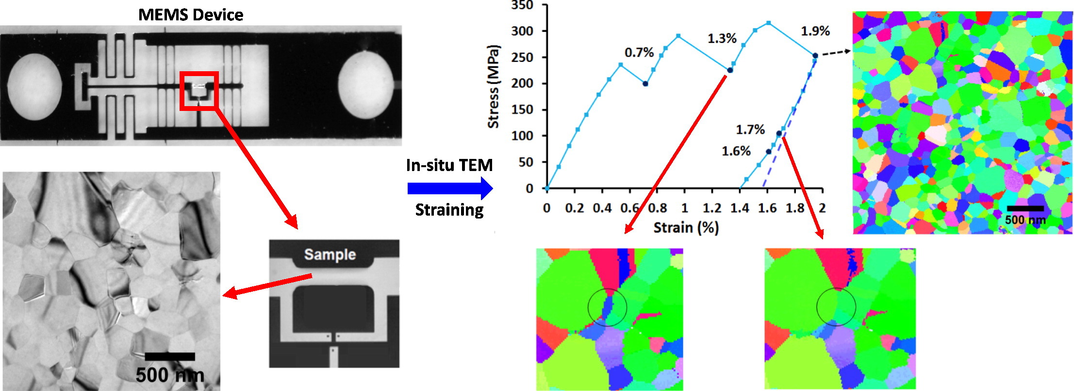
Izadi, E.; Darbal, A.; Sarkar, R.; Rajagopalan, J. Grain rotations in ultrafine-grained aluminum films studied using in situ TEM straining with automated crystal orientation mapping. Mater. Des., 113 (Jan. 2017), pp. 186-194; doi: 10.1016/j.matdes (2016)
" In-situ TEM straining allows probing deformation mechanisms of ultrafine-grained and nanocrystalline metals. While obtaining statistically meaningful information about microstructural changes using conventional bright-field/dark-field imaging or diffraction is time-consuming, automated crystal orientation mapping in TEM (ACOM-TEM) enables tracking orientation changes of hundreds of grains simultaneously. We use this technique to uncover extensive grain rotations during in-situ tensile deformation of a freestanding, ultrafine-grained aluminum film (thickness 200 nm, mean grain size 180 nm). During loading, both the fraction of grains that undergo rotations and the magnitude of their rotations increase with strain. The rotations are partially or fully reversible in a significant fraction of grains during unloading, leading to notable inelastic strain recovery. More surprisingly, the direction of rotation remains unchanged for a small fraction of grains during unloading, despite a sharp reduction in the applied stress. The ACOM-TEM measurements also provide evidence of reversible and irreversible grain/twin boundary migrations in the film. These microstructural observations point to a highly inhomogeneous and constantly evolving stress distribution in the film during both loading and unloading."
"A critical assumption underlying in-situ transmission electron microscopy studies is that the electron beam (e-beam) exposure does not fundamentally alter the intrinsic deformation behavior of the materials being probed. Here, we show that e-beam exposure causes increased dislocation activation and marked stress relaxation in aluminum and gold films spanning a range of thicknesses (80 – 400 nm) and grain sizes (50 – 220 nm). Furthermore, the e-beam induces anomalous sample necking, which unusually depends more on the e-beam diameter than intensity. Notably, the stress relaxation in both aluminum and gold occurs at beam energies well below their damage thresholds. More remarkably, the stress relaxation and/or sample necking is significantly more pronounced at lower accelerating voltages (120 kV versus 200 kV) in both the metals. These observations in aluminum and gold, two metals with highly dissimilar atomic weights and properties, indicate that e-beam exposure can cause anomalous behavior in a broad spectrum of nanostructured materials, and simultaneously suggest a strategy to minimize such artifacts."
 Optical micrograph of a typical MEMS device mounted on the TEM straining holder. (b) Optical micrograph of the MEMS device showing the force sensing beams. (c) Optical micrograph showing the freestanding Al sample and the strain and force measuring gauges. (d) Zoomed in image of the two strain sensing gauges x and y and the stationary force sensing gauge, z. The change in distance between gauges x and y gives the deformation on the sample while the change in distance between gauges x and z multiplied by the stiffness of the force sensing beams gives the force acting on the sample.")
Additional Publications
21. E. Izadi, A. Darbal, R. Sarkar, J. Rajagopalan, “Grain rotations in ultrafine-grained aluminum films studied using in situ TEM straining with automated crystal orientation mapping,” Materials and Design 113, 186–194, 2017.
20. R. Sarkar, C. Ebner, I. Izadi, C. Rentenberger, and J. Rajagopalan, “Revealing anelasticity and structural rearrangements in nanoscale metallic glass films using in situ TEM diffraction,” Materials Research Letters, 2016 DOI:10.1080/21663831.2016.1228709.
19. T. W. Sowers, R. Sarkar, S. E. Prameela, E. Izadi and J. Rajagopalan, “Capillary driven flow of polydimethylsiloxane in open rectangular micro channels,” Soft Matter 12, 5818-5823, 2016.
18. C. Ebner, R. Sarkar, J. Rajagopalan, and C. Rentenberger, “Local, atomic-level elastic strain measurements of metallic glass thin films by electron diffraction,” Ultramicroscopy 165, 51–58, 2016.
17. E. Izadi and J. Rajagopalan, “Texture dependent strain rate sensitivity of ultrafine-grained aluminum films,” Scripta Materialia 114, 65-69, 2016.
16. R. Sarkar, C. Rentenberger and J. Rajagopalan, “Electron beam induced artifacts during in situ TEM deformation of nanostructured metals,” Scientific Reports 5, 16345, 2015.
15. S. Singh, R. Sarkar, H.-X. Xie, C. Mayer, J. Rajagopalan, and N. Chawla, “Tensile behavior of single-crystal tin whiskers,” Journal of Electronic Materials 43, 978-982, 2014.
14. B. J. Williams, S. A. Anand, J. Rajagopalan and M. T. A. Saif, “A self-propelled biohybrid swimmer at low Reynolds number,” Nature Communications 5, 3081, 2014.
13. J. Rajagopalan and M. T. A. Saif, “Fabrication of freestanding 1-D PDMS microstructures using capillary micromolding,” Journal of Microelectromechanical Systems 22, 992-994, 2013.
12. J. Rajagopalan and M. T. A. Saif, “Effect of microstructural heterogeneity on the mechanical behavior of nanocrystalline metal films,” Journal of Materials Research 26, 2826-2832, 2011.
11. J. Rajagopalan and M. T. A. Saif, “MEMS sensors and microsystems for cell mechano-biology,” Journal of Micromechanics and Microengineering 21, 054002, 2011.
10. J. Rajagopalan, A. Tofangchi and M. T. A. Saif, “Linear, high-resolution bioMEMS force sensors with large measurement range,” Journal of Microelectromechanical Systems 19, 1380-1389, 2010.
9. W. Kang, J. Rajagopalan and M. T. A. Saif, “In situ uniaxial mechanical testing of small scale materials – a review,” Nanoscience and Nanotechnology Letters 2, 282-287, 2010.
8. J. Rajagopalan, A. Tofangchi and M. T. A. Saif, “Drosophila neurons actively regulate axonal tension in vivo,” Biophysical Journal 99, 3208-3215, 2010.
7. J. Rajagopalan, C. Rentenberger, P. H. Karnthaler, G. Dehm and M. T. A. Saif, “In situ TEM study of microplasticity and Bauschinger effect in nanocrystalline metals,” Acta Materialia 58, 4772-4782, 2010.
6. J. Rajagopalan, J. H. Han and M. T. A. Saif, “On plastic strain recovery in freestanding nanocrystalline metal thin films,” Scripta Materialia 59, 921-926, 2008.
5. J. Rajagopalan, J. H. Han and M. T. A. Saif, “Bauschinger effect in unpassivated freestanding nanoscale metal films,” Scripta Materialia 59, 734-737, 2008.
4. J. Rajagopalan, J. H. Han, and M. T. A. Saif, “Plastic deformation recovery in freestanding nanocrystalline aluminum and gold thin films,” Science 315, 1831-1834, 2007.
3. J. Rajagopalan and M. T. A. Saif, “A single degree of freedom model for thermoelastic damping,” Journal of Applied Mechanics 74, 461-468, 2007.
2. J. Rajagopalan, K. Balasubramaniam and C. V. Krishnamurthy, “A phase reconstruction algorithm for Lamb wave based structural health monitoring of anisotropic multilayered composite plates,” Journal of the Acoustical Society of America 119, 872-878, 2006.
1. J. Rajagopalan, K. Balasubramaniam and C. V. Krishnamurthy, “A single transmitter multi receiver (STMR) PZT array for guided ultrasonic wave based structural health monitoring of large isotropic plate structures,” Smart Materials and Structures 15, 1190-1196, 2006.
"To offer a state-of-the-art facility and processing capabilities open to all scientists and researchers in Australia and overseas to help realise outstanding research in materials and/or devices requiring sub-micrometre feature size for applications in, though not restricted to, photonics/opto-electronics."
The ANFF ACT is located at the Australian National University. Their facilities are based on photonic/electronic materials growth, processing and fabrication of devices including micro electro mechanical systems (MEMS). These facilities provide a range of capabilities and services for the micro/nanofabrication of photonic and related devices as well as the fabrication of waveguides and photonic crystals.
 Optoelectronic devices such as semiconductor lasers, photodetectors and modulators are widely used for communications, data storage, and medical applications. Further, photonic crystals, with their ability to confine light and guide and control its propagation, promise an entire suite of ultra-compact optical devices analogous to those of semiconductor electronics. Hence the node is internationally recognized for supporting both state-of-the-art research and proof-of-concept development for the industry.
ANFF-ACT also enjoys access to two well-known ANU research groups at the Laser Physics Centre and the Department of Electronic Materials Engineering. These groups bring expertise in the capabilities of high energy ion implantation, Si-etching, optical characterisation, and two metal organic chemical vapor deposition (MOCVD) reactors for the growth of III-V compound semiconductor multi- layers based on GaAs, AIGaAs, InGaAs, InP, InGaAsP, InAlGaAs, GaSb, InSb, and InGaAsN. These reactors enable the fabrication nanowires, quantum dots, quantum wells, strained layers, and devices.
Specialist fields:
Flagship facilities:
Please visit the lab's website for more information.
Publications
The Ringe Group was established in 2014 in the department of Materials Science and NanoEngineering (MSNE) at Rice University, Houston, TX, USA. Emilie Ringe and her...
The Ringe Group was established in 2014 in the department of Materials Science and NanoEngineering (MSNE) at Rice University, Houston, TX, USA. Emilie Ringe and her group focus on understanding and controlling light-matter interactions in small metallic nanoparticles for applications in biological sensing, enhanced spectroscopy, and light-driven heterogeneous catalysis.
By using correlated optical spectroscopy and electron microscopy tools, the group studies a phenomenon called localized surface plasmon resonance (LSPR), a type of light-matter interaction. LSPRs are a collective oscillation of the conduction electrons in a metal particle that leads to bright colors as well as strong electric fields at the surface of the particle. The resonance frequency changes with the surrounding environment, such that LSPR have exciting applications as nanosensors. Moreover, the strong fields can boost the catalytic activity of the metal surfaces.
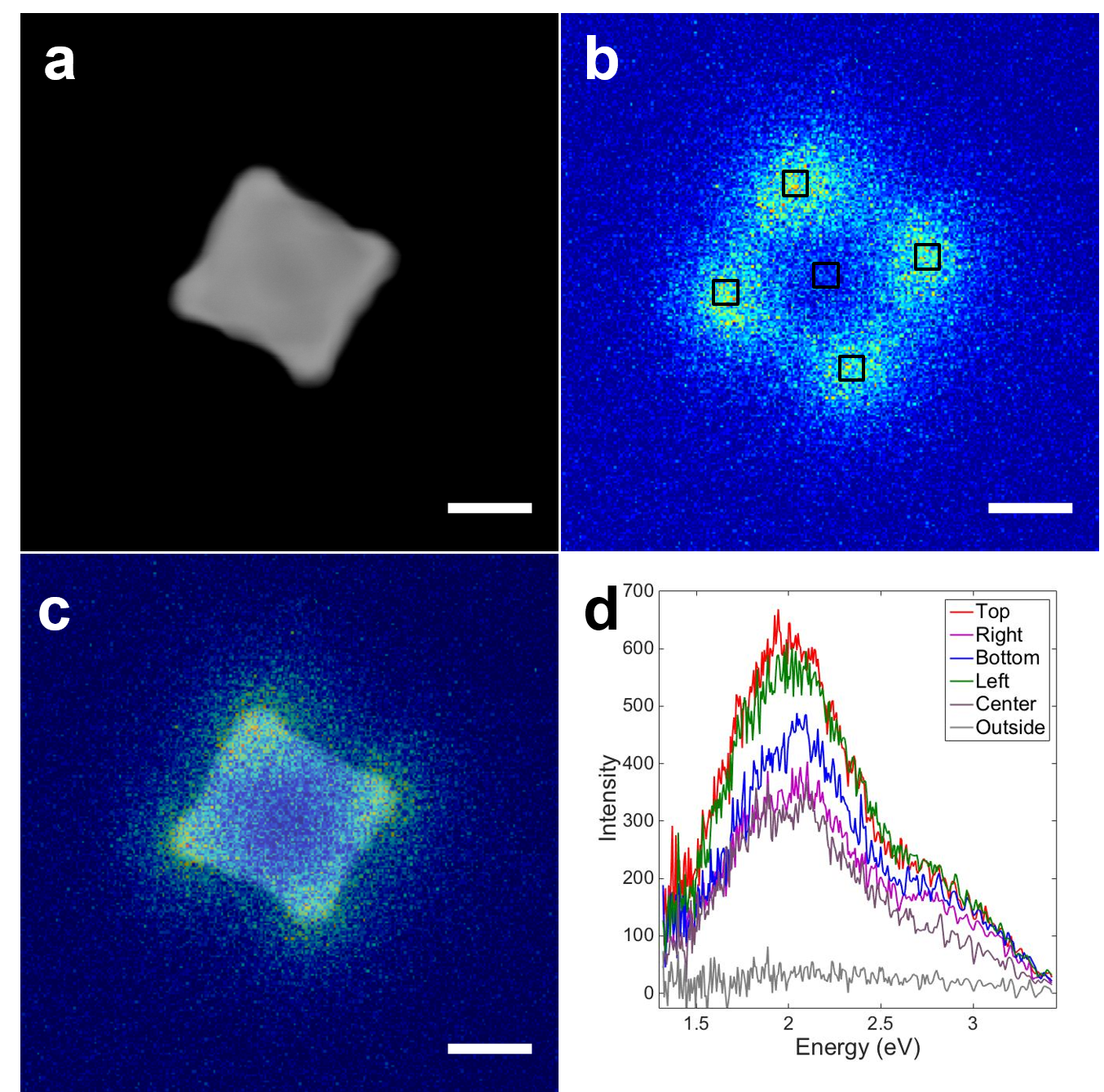
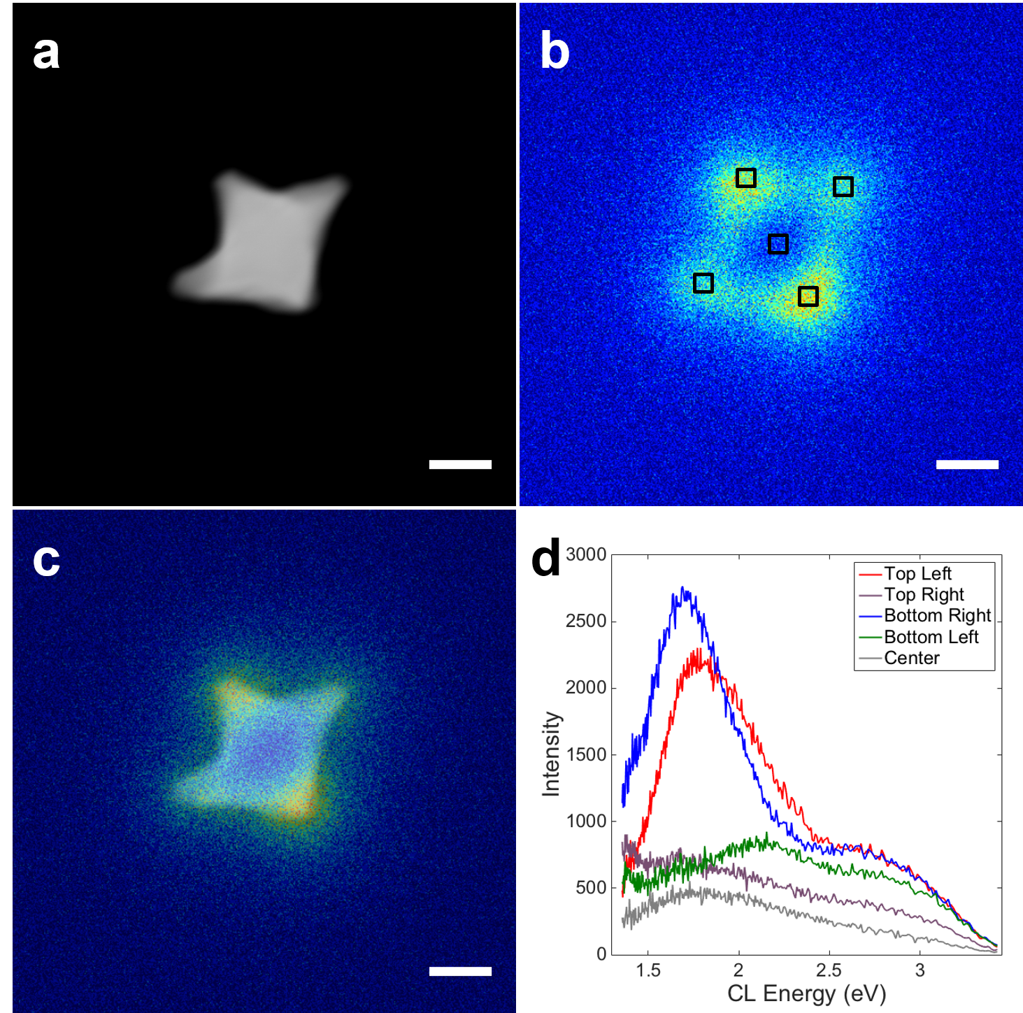
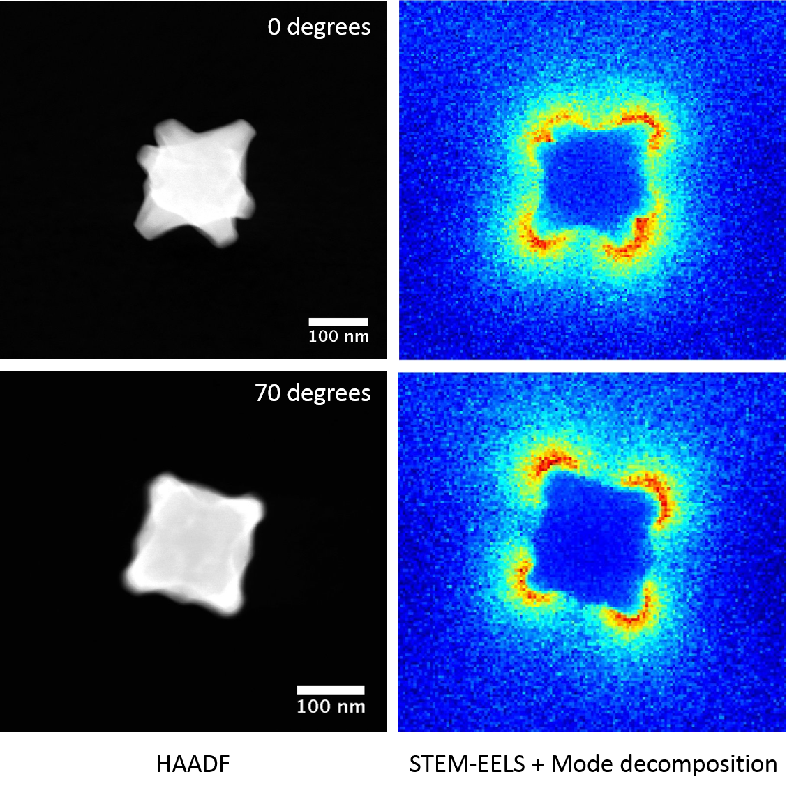
Both electrons and photons can interact with plasmon resonances, yielding either photons or electrons. Using electron energy loss spectroscopy (EELS) and cathodoluminescence (CL), techniques using an electron-based excitation and yielding an electron and a photon signal, respectively, the Ringe group studies the symmetry and localization of plasmon modes. Recently, work on Au/Pd nanoparticles has demonstrated that these alloy nanoparticles containing a poor plasmonic metal (Pd in this case) can nevertheless sustain a strong plasmonic response, enabling applications such as plasmon-enhanced photocatalysis and in-situ reaction monitoring and switching. Multiple size-dependent LSPRs and strong spatially localized fields at the Pd-rich tip of stellated particles were observed, where the composition is in fact least favorable for plasmon resonances. A strong substrate coupling was demonstrated via EELS tilt series and shows that Pd is fully participating in the resonances observed. Results are shown below.
Please visit the lab's website for more information.
Publications

The team at Electron Microscopy Group in Nano-Materials Research Institute of AIST aims to realize the characterization of nano-materials at a single...
The team at Electron Microscopy Group in Nano-Materials Research Institute of AIST aims to realize the characterization of nano-materials at a single atomic level by using the high-performance electron microscopy. They have developed the low-accelerating voltage transmission electron microscopy (TEM) and scanning TEM (STEM) equipped with high-order aberration correctors to visualize the atomic structures of low-dimensional materials such as carbon nanotubes, graphene, and transition-metal dichalcogenides as well as soft matters such as organic molecules and biomaterials. They have also focused on the chemical assignment of single atoms or molecules correlated to the atomic structures including defects and dopants by means of electron energy-loss spectroscopy (EELS).
How do atoms vibrate in graphene nanostructures?
Subtitle: Innovative new electron spectroscopy technique pushes the limits of Nanospectroscopy for materials design
In order to understand advanced materials like graphene nanostructures and optimize them for devices in nano-, opto- and quantum-technology it is crucial to understand how phonons – the vibration of atoms in solids – influence the materials’ properties. Researchers from the University of Vienna, the Advanced Institute of Science and Technology in Japan, the company JEOL and La Sapienza University in Rome have developed a method capable to measure all phonons existing in a nanostructured material. This is a breakthrough in the analysis of nanoscale functional materials and devices. With this pilot experiment using graphene nanostructures these researchers have shown the uniqueness of their approach, which will be published in the latest issue of Nature.

Important thermal, mechanical, optoelectronic and transport characteristics of materials are ruled by phonons: the propagating atomic vibrational waves. It is then inferable that the determination of such extended atomic vibrations is crucial for the optimization of nanoelectronic devices. The current available techniques use optical methods as well as inelastic electron-, x-ray- and neutron scattering. Despite its scientific importance in the last decade, none of these methods has been able to determine all phonons of a freestanding monolayer of two dimensional (2D) materials such as graphene and their local variations within a graphene nanoribbon, which are in turn used as active elements in nano- and optoelectronics.
The new limits of nanospectroscopy
An international research team of leading experts in electron spectroscopy led by Thomas Pichler at the University of Vienna, theoretical spectroscopy led by Francesco Mauri at La Sapienza University in Rome and electron microscopy led by Kazu Suenaga at the AIST Tsukuba in Japan, together with the Japanese company JEOL have presented an original method applying it to graphene nanostructures as model: ”high resolution electron spectroscopy inside an electron microscope with enough sensitivity to measure even an atomic monolayer”. In this way, they could for the first time determine all vibrational modes of freestanding graphene as well as the local extension of different vibrational modes in a graphene nanoribbon. This new method, which they called “large q mapping” opens entirely new possibilities to determine the spatial and momentum extension of phonons in all nanostructured as well as two-dimensional advanced materials. These experiments push the limits of nanospectroscopy approaching the limits of Heisenberg's uncertainty principle and demonstrate new possibilities to study local vibration modes at the nanometer scale down to individual monolayers.
New electron nanospectrometer as “tabletop” synchrotron
"The direct experimental proof of the full spatial and momentum resolved mapping of local vibrations of all materials including even monolayer 2D materials and nanoribbons will enable us to fully disentangle different vibration modes and their momentum transfers at non-perfect structures such as edges or defects, which are extremely important to understand and optimize the local properties of a material", explains one of the leading authors, Ryosuke Senga.
This study of “High q-Mapping Of Vibrations” in the electron microscope opens a new pathway of nanospectroscopy of all materials combining spatial and momentum resolved measurements. This has been the biggest challenge regarding the combination of microscopy and spectroscopy, since the spatial and momentum resolutions are compensated due to the limit of Heisenberg's uncertainty principle. "We believe that our methodology will boost vast research in material science and will push high-resolution electron spectroscopy in electron microscopy to the next level, to be envisaged as a true tabletop synchrotron", says Thomas Pichler from the University of Vienna.
The work was supported by FWF, the EU, and JSPS.