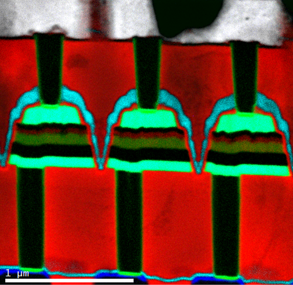
Cathodoluminescence image of paint pigment

Cathodoluminescence image of paint pigment
Data courtesy of Prof. Nicholas Leventis, Chemistry Department, Missouri University of Science and Technology

Cathodoluminescence image of paint pigment sample prepared with Ilion II and imaged with MonoCL4™ system.

Polymer aerogel

Polymer aerogel

Electrical activity of grain boundaries in polycrystalline silicon solar cells

Electrical activity of grain boundaries in polycrystalline silicon solar cells
R. Johnson

A quantified EBIC map of a polycrystalline silicon solar cell. Several grain boundary segments are revealed to be electrically active (high recombination rate) and appear dark in the EBIC map (indicated by red arrows) while some appear to be electrically inactive (indicated by green arrow). Electrically active defects reduce the overall efficiency of the solar cell.

Electrical activity of grain boundaries in CdTe solar cell

Electrical activity of grain boundaries in CdTe solar cell
Data courtesy of Dr. J. Poplawsky, Oak Ridge National Laboratory

(a) Quantitative EBIC contrast map from the cross section of a CdTe/CdS solar cell after CdCl2 and Cu treatment; the intensity scale shows the EBIC contrast number (EBIC current normalized by the electron beam current).

Identify the position of p-n junction in a device

Identify the position of p-n junction in a device

Overlay of the secondary electron (red) and EBIC (blue) images from a GaAs amplifier. The EBIC signal reveals the position of the p-n junction and allows quantitative analysis of the built-in electric field.

Zeolite beta low dose image series

Zeolite beta low dose image series
Sample courtesy of Prof. D.L. Zhang at Jilin University, China.

(a) – (c) Zeolite beta electron dose series of 0.5, 2, and 8 e-/pixel; (d) – (f) corresponding FFT images. As dose increases image quality improves and more reflections can be seen in the FFT image. 

Zeolite beta low dose images

Sample courtesy of Prof. D.L. Zhang at Jilin University, China.
(a) A single sub-image frame (0.125 s exposure) of zeolite beta along [100] zone axis. Electron dose for this image is 0.5 e-/pixel or 11 e-/A2; (b) Enlarged area of the outlined in (a); (c) FFT image of (b). The d-spacing of (0, 0, 16) is 1.7 A.

Nano-beam electron diffraction full 2D strain mapping

Data courtesy V. B. Ozdol et al., National Center for Electron Microscopy, Lawrence Berkeley National Laboratory and Department of Materials Science and Engineering, University of California, Berkeley, California.
a) HAADF image of a GaAs/GaAsP multilayer laminate; b) Integrated diffraction pattern of the superlattice structure along the [011] zone axis; c) Virtual BF image extracted from 4D data cube quantifying strain down to 1.2 nm resolution in full 2D area in eyy; d) exx strain for same area shown.

Correlating microstructure with luminescence properties at the nanoscale

Correlating microstructure with luminescence properties at the nanoscale
Data courtesy of Dr. R. Williams, Ohio State University

Cathodoluminescence analysis of a GaN/AlN nanowire in STEM (a) Dark field STEM image, (b) cathodoluminescence spectrum-image acquired from the region indicated by the green rectangle in (a), (c) A cathodoluminescence spectrum extracted from the spectrum-image, and (d) a projection of the cathodoluminescence spectrum with the information along the y-axis (radial direction) of the nanowire summed into a single value. The resultant data set shows the spectral information as a function of position along the nanowire length.

Dislocation density analysis in semiconductors

Dislocation density analysis in semiconductors

Panchromatic cathodoluminescence image of bulk GaN sample. Dark spots (some indicated by blue arrows) correspond to threading dislocations. A dislocation density of 5 x 105 cm-2 was measured. Acquisition time = 30 s. The corresponding secondary electron image (revealing topography) showed no contrast.

Pages