Multi-convergence-angle ptychography with simultaneous strong contrast and high resolution
arXiv
2024
There is considerable interest in emerging materials due to their extreme strength, flexibility, optical transparency and thermal conductivity. Prior to incorporation into new products, it is crucial to understand, employ and predict failures in new materials, surfaces and interfaces, nanostructures, clusters, and materials under various extreme conditions with atomic resolution. In particular, compositional analysis is a valuable tool because it enables researchers to understand the structure–property relationships for each component and their synergistic behaviors to better characterize significant changes in the material structure and elemental distribution. Useful compositional attributes to understand include:
To adequately characterize and understand the compositional material of your product or specimen, you must first ensure each specimen is of the highest quality to resolve the material interface and properly controlled so you manipulate it, when necessary, under environmental stimuli. Once prepared, several techniques are available to better understand the composition of material(s).
|
Electron energy loss spectroscopy (EELS) Delivers atomic-scale insights into elemental composition and chemical bonding—enabling a deeper understanding of material properties to advance fundamental research and discovery. Includes energy-filtered TEM (EFTEM). Elevate your EELS at EELS.info. |
Energy dispersive x-ray spectroscopy (EDS/EDX) Facilitates rapid, reliable elemental analysis by detecting characteristic x-rays emitted from a sample, allowing researchers to identify and quantify major, minor, and trace elements across a wide range of materials. |
|
Integrates EELS, EDS, 4D STEM, and more to deliver rich, correlated insights—advancing the understanding of complex, dynamic nanoscale phenomena. |
Delivers high-resolution visualization of biological and inorganic specimens, enabling researchers to study ultrastructure, material growth, and failure mechanisms with exceptional clarity. |
|
Captures real-time nanoscale dynamics under controlled stimuli to uncover fundamental mechanisms and accelerate scientific discovery. |
Integrated SEM Combines EDS, EBSD, CL, BSE, and WDS into unified platforms—delivering comprehensive, high-resolution insights that streamline workflows and deepen understanding of complex materials. |
|
Wavelength dispersive x-ray spectroscopy (WDS) Offers high spectral resolution and sensitivity, enabling precise identification and quantification of trace and light elements in complex samples—especially where overlapping x-ray lines challenge other techniques. |
Visit chemical analysis or metals and alloys learn about related applications.
What elements are within the sample?
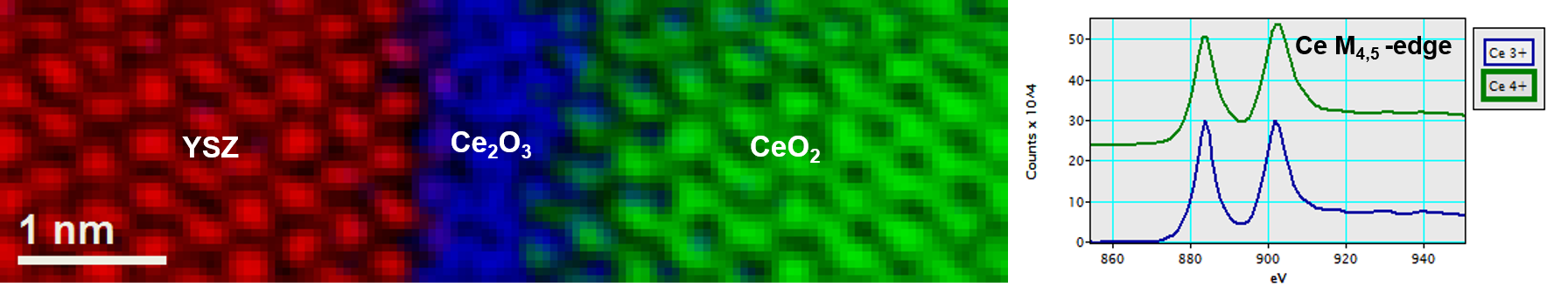
In this example, Y and Zr edges were acquired and mapped using the EELS technique, while Ce3,4 atomic maps were obtained using MLLS fitting. The total acquisition time for this image was 244 s and the entire spectra was acquired in a single range mode of 400 – 2400 eV. Beam current was 125 pA with an energy resolution of 3 eV.
AuGeNi ohmic contacts are widely used as they show a low contact resistivity and are typically compatible with the fabrication of III-V MOSFET devices. However, they have the drawback of poor uniformity due to diffusion of the Au into the III-V substrate. This diffusion is dependent on temperature used during the annealing process after deposition of Au, Ge and Ni. Using EELS and EFTEM techniques, you can determine how the material present and degree of roughness at the interface with the III-V substrate influence device performance. Sample courtesy of University of Glasgow Microscope courtesy of Professor Ray Carpente at Arizona State University, Tempe, AZ. Acknowledgement to Dr. Toshiro Aoki at Jeol USA (now at ASU) for helping set up the microscope for the experiment.

Measure composition uniformity
You can distinguish variations in material composition between grains using cathodoluminescence. In this example, variations are shown as a change in color, with the excess of vacancy point defects at grain boundaries highlighted in blue. Image a) shows the secondary electron image of a Cu0.8In0.2AgSe2 film. Image b) shows the overlaid monochromatic cathodoluminescence images: 1.181 eV emission (blue), 1.121 eV (green), and 1.033 eV (red). Images courtesy of A.R. Aquino Gonzales, Ph.D. Dissertation, University of Illinois.
