Nondeterministic dynamics in the η-to-θ phase transition of alumina nanoparticles
Science
2025
Metals and alloys are critical building blocks of many products, from nanomaterials to architectural structures. The specific composition of an individual metal or alloy is critical to achieve a desired strength, microstructure, or corrosion resistance of a material. To achieve this specific composition, researchers will study topographical or microstructural features to better understand the alloy composition of raw materials, conformance to a purity specification, identify alloys used to make a specific component, or investigate foreign contaminants during component failure analysis. Useful information to better understand these attributes includes:
To adequately characterize and understand metals and alloys, you must first ensure each specimen is of the highest quality to resolve the material interface and properly controlled so you manipulate it, when necessary, under environmental stimuli. Once prepared, several techniques are available to better understand material complexities and failures to improve device performance.
|
Electron backscatter diffraction (EBSD) Allows detailed microstructural analysis by mapping crystal orientations, phases, and grain boundaries, helping researchers understand material properties, deformation, and failure mechanisms at the microscale. |
Energy dispersive x-ray spectroscopy (EDS/EDX) Facilitates rapid, reliable elemental analysis by detecting characteristic x-rays emitted from a sample, allowing researchers to identify and quantify major, minor, and trace elements across a wide range of materials. |
|
Electron energy loss spectroscopy (EELS) Delivers atomic-scale insights into elemental composition and chemical bonding—enabling a deeper understanding of material properties to advance fundamental research and discovery. Includes energy-filtered TEM (EFTEM). Elevate your EELS at EELS.info. |
Integrates EELS, EDS, 4D STEM, and more to deliver rich, correlated insights—advancing the understanding of complex, dynamic nanoscale phenomena. |
|
Delivers high-resolution visualization of biological and inorganic specimens, enabling researchers to study ultrastructure, material growth, and failure mechanisms with exceptional clarity. |
Captures real-time nanoscale dynamics under controlled stimuli to uncover fundamental mechanisms and accelerate scientific discovery. |
|
Integrated SEM Combines EDS, EBSD, CL, BSE, and WDS into unified platforms—delivering comprehensive, high-resolution insights that streamline workflows and deepen understanding of complex materials. |
Micro x-ray fluorescence (Micro-XRF) Delivers high-resolution, non-destructive elemental analysis—ideal for layered, sensitive, or irregular samples. |
|
Wavelength dispersive x-ray spectroscopy (WDS) Offers high spectral resolution and sensitivity, enabling precise identification and quantification of trace and light elements in complex samples—especially where overlapping x-ray lines challenge other techniques. |
Visit compositional or chemical analysis to learn more about related applications.
Adequate preparation for compositional analysis
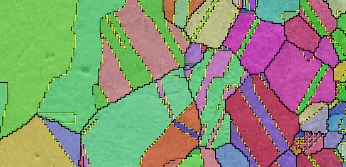
During an EBSD experiment, surface damage can significantly alter diffraction patterns you obtain from crystalline samples. Therefore it is important for you to use an electropolishing tool, such as the PECS II system, to ensure your specimen's surface is sufficiently smooth to prevent shadow formation in your diffraction pattern. The image below shows that the PECS II system was able to preserve the integrity of a highly stressed Zircaloy 2 alloy sample so that you can distinguish high resolution boundaries of an IPFZ map with a 1 x 0.7 mm field of view of a . Results courtesy of Department of Materials, University of Oxford. Professor Angus Wilkinson and Dr. Hamidreza Abdolvand. Sample prepared with a PECS II system. Data acquired on a Zeiss Compact Merlin equipped with a Bruker Quantax EBSD System.

Discriminate fine sample details
Specimen motion, drift and irradiation damage are common challenges you may encounter with sensitive samples or when you measure sample activity over time. When you employ a live drift correction to automatically and constantly remove the shift between adjacent images to eliminate most or all of the artifact and resolution loss. Below image shows highly sensitive zeolite sample at 4k x 4k resolution that were acquired using the OneView® camera.
. Drift correction is on (right). Both images were taken with 1 s of exposure. Chevron SSZ-57 zeolite (4k x 4k)")
Capture sintering, recrystallization and phase transformations
Below shows gold nanoparticles sintering during an in-situ experiment. See how you can use the OneView camera to record individual images at full resolution, so every frame in these video is a 4k x 4k high resolution image. This enables post-processing later – whether you’re extracting individual images, applying post-capture drift correction or creating movies from all or just a portion of the images. You are able to capture reactions at extremely high temporal and spatial resolution. Below, on the far left the movie shows full field of view (35 x 35 nm2), and skipped 5 frames, 1k x 1k. The middle movie is cropped to region of interest (ROI), bin x1, and skipped 3 frames. The far right movie has been cropped to ROI and binned x1.
Image on left is an EBSD map of bronze specimen recrystallization taken in situ at 800 ºC. Image on the right shows the ability to study dynamic EBSD phase transformations within the tight geometry restrictions of a SEM.