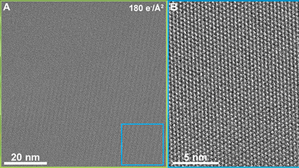
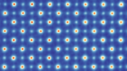
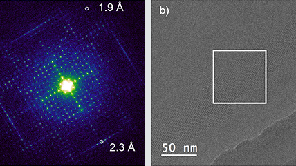
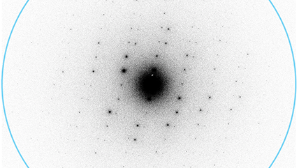
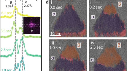
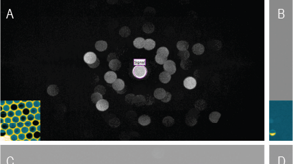
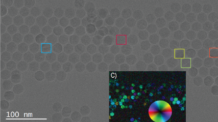
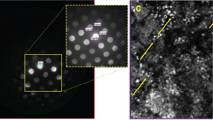
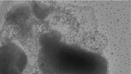
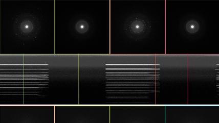
Multi-convergence-angle ptychography with simultaneous strong contrast and high resolution
Mao, W.; Zhang, W.; Huang, C.; Zhou, L.; Kim, J. S.; Gao, S.; Lei, Y.; Wu, X.; Hu, Y.; Pei, X.; Fang, W.; Liu, X.; Song, J.; Fan, C.; Nie, Y.; Kirkland, A. I.; Wang, P.
Nanostructured 3C-SiC on Si by a network of (111) platelets: A fully textured film generated by intrinsic growth anisotropy
Physical Chemistry Chemical Physics
Vanacore, G. M.;Chrastina, D.; Scalise, E.; Barbisan, L.; Ballabio, A.; Mauceri, M.; Via, F. L.; Capitani, G.; Crippa, D.; Marzegalli, A.; Bergamaschini. R.; Miglio. L.
Deagglomeration of DNA nanomedicine carriers using controlled ultrasonication
Ultrasonics Sonochemistry
Hinchliffe, B. A.; Turner, P.; J. H. Cant, D.; De Santis, E.; Aggarwal, P.; Harris, R.; Templeton, D.; Shard, A. G.; Hodnett, M.; Minelli, C.
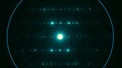
Three-dimensional electron ptychography of organic–inorganic hybrid nanostructures
Ding, Z.; Gao, S.; Fang, W.; Huang, C.; Zhou, L.; Pei, X.; Liu, X.; Pan, X.; Fan, C.; Kirkland, A. I.; Wang, P.
Phosphorylation of SAMHD1 Thr592 increases C-terminal domain dynamics, tetramer dissociation and ssDNA binding kinetics
Orris, B.; Huynh, K. W.; Ammirati, M.; Han, S.; Bolaños, B.; Carmody, J.; Petroski, M. D.; Bosbach, B.; Shields, D. J.; Stivers, J. T.
Metastable hexagonal close-packed palladium hydride in liquid cell TEM
Hong, J.; Bae, J. -H.; Jo, H.; Park, H. -Y.; Lee, S.; Hong, S. J.; Chun, H.; Cho, M. K.; Kim, J.; Kim, J.; Son, Y.; Jin, H.; Suh, J. -Y.; Kim, S. -C.; Roh, H. -K.; Lee, K. H.; Kim, H. -S.; Chung, K. Y.; Yoon, C. W.; Lee, K.; Kim, S. H.; Ahn, J. -P.; Baik, H.; Kim, G. H.; Han, B.; Jin, S.; Hyeon, T.; Park, J.; Son, C. Y.; Yang, Y.; Lee, Y. -S.; Yoo, S. J.; Chun, D. W.
Potential nanoscale sources of decoherence in niobium based transmon Qubit architectures
Murthy, A. A.; Das, P. M.; Ribet, S. M.; Kopas, C.; Lee, J.; Reagor, M. J.; Zhou, L.; Kramer, M. J.; Hersam, M. C.; Checchin, M.; Grassellino, A.; dos Reis, R.; Dravid, V. P.; Romanenko, A.
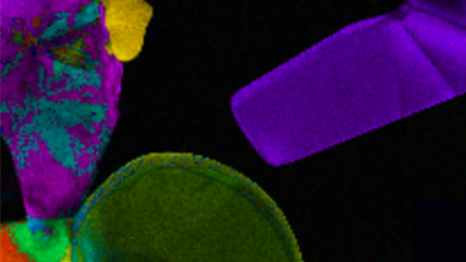
High-density switchable skyrmion-like polar nanodomains integrated on silicon
Han, L.; Addiego, C.; Prokhorenko, S.; Wang, M.; Fu, H.; Nahas, Y.; Yan, X.; Cai, S.; Wei, T.; Fang, Y.; Liu, H.; Ji, D.; Guo, W.; Gu, Z.; Yang, Y.; Wang, P.; Bellaiche, L.; Chen, Y.; Wu, D.; Nie, Y.; Pan, X.
The giant Mimivirus 1.2 Mb genome is elegantly organized into a 30 nm helical protein shield
Villalta, A.; Schmitt, A.; Estrozi, L. F.; Quemin, E. R. J.; Alempic, J. -M.; Lartigue, A.; Pražák, V.; Belmudes, L.; Vasishtan, D.; Colmant, A. M. G.; Honoré, F. A.; Couté, Y.; Grünewald, K.; Abergel, C.
Suspension electrolyte with modified Li+ solvation environment for lithium metal batteries
Kim, M. S.; Zhang, Z.; Rudnicki, P. E.; Yu, Z.; Wang, J.; Wang, H.; Oyakhire, S. T.; Chen, Y.; Kim, S. C.; Zhang, W.; Boyle, D. T.; Kong, X.; Xu, R.; Huang, Z.; Huang, W.; Bent, S. F.; Wang, L. -W.; Qin, J.; Bao, Z.; Cui , Y.
Rational solvent molecule tuning for high-performance lithium metal battery electrolytes
Yu, Z.; Rudnicki, P. E.; Zhang, Z.; Huang, Z.; Celik, H.; Oyakhire, S. T.; Chen, Y.; Kong, X.; Kim, S. C.; Xiao, X.; Wang, H.; Zheng, Y.; Kamat, G. A.; Kim, M. S.; Bent, S. F.; Qin, J.; Cui, Y.; Bao, Z.
Capturing the swelling of solid-electrolyte interphase in lithium metal batteries
Zhang, Z.; Li, Y.; Xu, R.; Zhou, W.; Li, Y.; Oyakhire, S. T.; Wu, Y.; Xu, J.; Wang, H.; Yu, Z.; Boyle, D. T.; Huang, W.; Ye, Y.; Chen, H.; Wan, J.; Bao, Z.; Chiu, W.; Cui, Y.
Electric field control of chirality
Behera, P.; May, M. A.; Gomez-Ortiz, F.; Susarla, S.; Das, S.; Nelson, C. T.; Caretta, L.; Hsu, S. -L.; McCarter, M. R.; Savitzky, B. H.; Barnard, E. S.; Raja, A.; Hong, Z.; Garcia-Fernandez, P.; Lovesey, S. W.; Van der Laan, G.; Ercius, P.; Ophus, C.; Martin, L. W.; Junquera, J.; Raschke, M. B.; Ramesh, R.
De novo synthesis of free-standing flexible 2-D intercalated nanofilm uniform over tens of cm2
Ravat, P.; Uchida, H.; Sekine, R.; Kamei, K.; Yamamoto, A.; Konovalov, O.; Tanaka, M.; Yamada, T.; Harano, K.; Nakamura, E.
SINGLE: Atomic-resolution structure identification of nanocrystals by graphene liquid cell EM
Reboul, C. F.; Heo, J.; Machello, C.; Kiesewetter, S.; Kim, B. H.; Kim, S.; Elmlund, D.; Ercius, P.; Park, J.; Elmlund, H.
Identification of viral particles in the apoplast of Nicotiana benthamiana leaves infected by potato virus X
Molecular Plant Pathology
Hu, S.; Yin, Y.; Chen, B.; Lin, Q.; Tian, Y.; Song, X.; Peng, J.; Zheng, H.; Rao, S.; Wu, G.; Mo, X.; Yan, F.; Chen, J.; Lu, Y.
Complete mapping of mutations to the SARS-CoV-2 spike receptor-binding domain that escape antibody recognition
Greaney, A. J.; Starr, T. N.; Gilchuk, P.; Zost, S. J.; Binshtein, E.; Loes, A. N.; Hilton, S. K.; Huddleston, J.; Eguia, R.; Crawford, K. H. D.; Dingens, A. S.; Nargi, R. S.; Sutton, R. E.; Suryadevara, N.; Rothlauf, P. W.; Liu, Z.; Whelan, S. P. J.; Carnahan, R. H.; Bloom, J. D.
Mechanism of SARS-CoV-2 polymerase stalling by remdesivir
Kokic, G.; Hillen, H. S.; Tegunov, D.; Dienemann, C.; Seitz, F.; Schmitzova, J.; Farnung, L.; Siewert, A.; Höbartner, C.; Cramer, P.
Development and structural basis of a two-MAb cocktail for treating SARS-CoV-2 infections
Zhang, C.; Wang, Y.; Zhu, Y.; Liu, C.; Gu, C.; Xu, S.; Wang, Y.; Zhou, Y.; Wang, Y.; Han, W.; Hong, X.; Yang, Y.; Zhang, X.; Wang, T.; Xu, C.; Hong, Q.; Wang, S.; Zhao, Q.; Qiao, W.; Zang, J.; Kong, L.; Wang, F.; Wang, H.; Qu, D.; Lavillette, D.; Tang, H.; Deng, Q.; Xie, Y.; Cong, Y.; Huang, Z.
Cryo-EM structure of an extended SARS-CoV-2 replication and transcription complex reveals an intermediate state in cap synthesis
Yan, L.; Ge, J.; Zheng, L.; Zhang, Y.; Gao, Y.; Wang, T.; Huang, Y.; Yang, Y.; Gao, S.; Li, M.; Liu, Z.; Wang, H.; Li, Y.; Chen, Y.; Guddat, L. W.; Wang, Q.; Rao, Z.; Lou, Z.
Conformational dynamics of SARS-CoV-2 trimeric spike glycoprotein in complex with receptor ACE2 revealed by cryo-EM
Xu, C.; Wang, Y.; Liu, C.; Zhang, C.; Han, W.; Hong, X.; Wang, Y.; Hong, Q.; Wang, S.; Zhao, Q.; Wang, Y.; Yang, Y.; Chen, K.; Zheng, W.; Kong, L.; Wang, F.; Zuo, Q.; Huang, Z.; Cong, Y.
Nonstructural protein 1 of SARS-CoV-2 is a potent pathogenicity factor redirecting host protein synthesis machinery toward viral RNA
Yuan, S.; Peng, L.; Park, J. J.; Hu, Y.; Devarkar, S. C.; Dong, M. B.; Shen, Q.; Wu, S.; Chen, S.; Lomakin, I. B.; Xiong, Y.
Cryo-EM structures of SARS-CoV-2 spike without and with ACE2 reveal a pH-dependent switch to mediate endosomal positioning of receptor-binding domains
Zhou, T.; Tsybovsky, Y.; Gorman, J.; Rapp, M.; Cerutti, G.; Chuang, G. -Y.; Katsamba, P. S.; Sampson, J. M.; Schön, A.; Bimela, J.; Boyington, J. C.; Nazzari, A.; Olia, A. S.; Shi, W.; Sastry, M.; Stephens, T.; Stuckey, J.; Teng, I. -T.; Kwong, P. D
Electronically coupled 2D polymer/MoS2 heterostructures
Journal of American Chemical Society
Balch, H. B., Evans, A. M., Dasari, R. R., Li, H., Li, R., Thomas, S., Wang, Q., Bisbey, R. P., Slicker, K., Castano, I., Xun, S., Jiang, L., Zhu, C., Gianneschi, N., Ralph, D. C., Brédas, J-L., Marder, S. R., Dichtel, W. R., Wang, F.
De novo design of potent and resilient hACE2 decoys to neutralize SARS-CoV-2
Linsky, T. W.; Vergara, R.; Codina, N.; Nelson, J. W.; Walker, M. J.; Su, W.; Barnes, C. O.; Hsiang, T. -Y.; Esser-Nobis, K.; Yu, K.; Reneer, B.; Hou, Y. J.; Priya, T.; Mitsumoto, M.; Pong, A.; Lau, Y.; Mason, M. L.; Chen, J.; Chen, A.; Berrocal, T.; Peng, H.; Clairmont, N. S.; Castellanos, J.; Lin, Y. -R..; Josephson-Day, A.; Baric, R. S.; Fuller, D. H.; Walkey, C. D.; Ross, T. M.; Swanson, R.; Bjorkman, P. J.; Gale Jr., M.; Blancas-Mejia, L. M.; Yen, H. -L.; Silva, D. -A.
Rational development of a human antibody cocktail that deploys multiple functions to confer Pan-SARS-CoVs protection
Yao, H.; Sun, Y.; Deng, Y. -Q.; Wang, N.; Tan, Y.; Zhang, N. -N.; Li, X. -F.; Kong, C.; Xu, Y. -P.; Chen, Q.; Cao, T. -S.; Zhao, H.; Yan, X.; Cao, L.; Lv, Z.; Zhu, D.; Feng, R.; Wu, N.; Zhang, W.; Hu, Y.; Chen, K.; Zhang, R. -R.; Lv, Q.; Sun, S.; Zhou, Y.; Yan, R.; Yang, G.; Sun, X.; Liu, C.; Lu, X.; Cheng, L.; Qiu, H.; Huang, X. -Y.; Weng, T.; Shi, D.; Jiang, W.; Shao, J.; Wang, L.; Zhang, J.; Jiang, T.; Lang, G.; Qin, C. -F.; Li, L.; Wang, X.
Structure-based development of human antibody cocktails against SARS-CoV-2
Wang, N.; Sun, Y.; Feng, R.; Wang, Y.; Guo, Y.; Zhang, L.; Deng, Y. -Q.; Wang, L.; Cui, Z.; Cao, L.; Zhang, Y. -J.; Li, W.; Zhu, F. -C.; Qin, C. -F.; Wang, X.
Structural analysis of full-length SARS-CoV-2 spike protein from an advanced vaccine candidate
Bangaru, S.; Ozorowski, G.; Turner, H. L.; Antanasijevic, A.; Huang, D.; Wang, X.; Torres, J. L.; Diedrich, J. K.; Tian, J. -H.; Portnoff, A. D.; Patel, N.; Massare, M. J.; Yates III, J. R.; Nemazee, D.; Paulson, J. C.; Glenn, G.; Smith, G.; Ward, A. B.
Ultrapotent human antibodies protect against SARS-CoV-2 challenge via multiple mechanisms
Tortorici, M. A.; Beltramello, M.; Lempp, F. A.; Pinto, D.; Dang, H. V.; Rosen, L. E.; McCallum, M.; Bowen, J.; Minola, A.; Jaconi, S.; Zatta, F.; De Marco, A.; Guarino, B.; Bianchi, S.; Lauron, E. J.; Tucker, H.; Zhou, J.; Peter, A.; Havenar-Daughton, C.; Wojcechowskyj, J. A.; Case, J. B.; Chen, R. E.; Kaiser, H.; Montiel-Ruiz, M.; Meury, M.; Czudnochowski, N.; Spreafico, R.; Dillen, J.; Ng, C.; Sprugasci, N.; Culap, K.; Benigni, F.; Abdelnabi, R.; Foo, S. -Y. C.; Schmid, M. A.; Cameroni, E.; Riva, A.; Gabrieli, A.; Galli, M.; Pizzuto. M. S.; Neyts, J.; Diamond, M. S.; Virgin, H. W.; Snell, G.; Corti, D.; Fink, K.; Veesler, D.;
Architecture of a SARS-CoV-2 mini replication and transcription complex
Yan, L.; Zhang, Y.; Ge, J.; Zheng, L.; Gao, Y.; Wang, T.; Jia, Z.; Wang, H.; Huang, Y.; Li, M.; Wang, Q.; Ra, Z.; Lou, Z.
Structurally resolved SARS-CoV-2 antibody shows high efficacy in severely infected hamsters and provides a potent cocktail pairing strategy
Du, S.; Cao, Y.; Zhu, Q.; Yu, P.; Qi, F.; Wang, G.; Du, X.; Bao, L.; Deng, W.; Zhu, H.; Liu, J.; Nie, J.; Zheng, Y.; Liang, H.; Liu, R.; Gong, S.; Xu, H.; Yisimayi, A.; Qin, C.
Mapping neutralizing and immunodominant sites on the SARS-CoV-2 spike receptor-binding domain by structure-guided high-resolution serology
Piccoli, L.; Park, Y. -J.; Tortorici, M. A.; Czudnochowski, N.; Walls, A. C.; Beltramello, M.; Silacci-Fregni, C.; Pinto, D.; Rosen, L. E.; Bowen, J. E.; Acton, O. J.; Jaconi, S.; Guarino, B.; Minola, A.; Zatta, F.; Sprugasci, N.; Bassi, J.; Peter, A.; De Marco, A.; Nix, J. C.; Mele, F.; Jovic, S.; Rodriguez, B. F.; Gupta, S. V.; Jin, F.; Piumatti, G.; Presti, G. L.; Pellanda, A. F.; Biggiogero, M.; Tarkowski, M.; Pizzuto, M. S.; Cameroni, E.; Havenar-Daughton, C.; Smithey, M.; Hong, D.; Lepori, V.; Albanese, E.; Ceschi, A.; Bernasconi, E.; Elzi, L.; Ferrari, P.; Garzoni, C.; Riva, A.; Snell, G.; Sallusto, F.; Fink, K.; Virgin, H. W.; Lanzavecchia, A.; Corti, D.; Veesler, D.
Engineered trimeric ACE2 binds viral spike protein and locks it in “Three-up” conformation to potently inhibit SARS-CoV-2 infection
Guo, L.; Bi, W.; Wang, X.; Xu, W.; Yan, R.; Zhang, Y.; Zhao, K.; Li, Y.; Zhang, M.; Cai, X.; Jiang, S.; Xie, Y.; Zhou, Q.; Lu, L.; Dang, B.
Cathode-electrolyte interphase in lithium batteries revealed by cryogenic electron microscopy
Zhang, Z.; Yang, J.; Huang, W.; Wang, H.; Zhou, W.; Li, Y.; Li, Y.; Xu, J.; Huang, W.; Chiu, W.
Free fatty acid binding pocket in the locked structure of SARS-CoV-2 spike protein
Toelzer, C.; Gupta, K.; Yadav, S. K. N.: Borucu, U.; Davidson, A. D.; Williamson, M. K.; Shoemark, D. K.; Garzoni, F.; Staufer, O.; Milligan, R.; Capin, J.; Mulholland, A. J.; Spatz, J.; Fitzgerald, D.; Berger, I.; Schaffitzel, C.
An ultrapotent synthetic nanobody neutralizes SARS-CoV-2 by stabilizing inactive spike
Schoof, M.; Faust, B.; Saunders, R. A.; Sangwan, S.; Rezelj, V.; Hoppe, N.; Boone, M.; Billesbølle, C. B.; Puchades, C.; Azumaya, C. M.; Kratochvil, H. T.; Zimanyi, M.; Deshpande, I.; Liang, J.; Dickinson, S.; Nguyen, H. C.; Chio, C. M.; Merz, G. E.; Thompson, M. C.; Diwanji, D.; Schaefer, K.; Anand, A. A.; Dobzinski, N.; Zha, B. S.; Simoneau, C. R.; Leon, K.; White, K. M.; Chio, U. S.; Gupta, M.; Jin, M.; Li, F.; Liu, Y.; Zhang, K.; Bulkley, D.; Sun, M.; Smith, A. M.; Rizo, A. N.; Moss, F.; Brilot, A. F.; Pourmal, S.; Trenker, R.; Pospiech, T.; Gupta, S.; Barsi-Rhyne, B.; Belyy, V.; Barile-Hill, A. W.; Nock, S.; Liu, Y.; Krogan, N. J.; Ralston, C. Y.; Swaney, D. L.; García-Sastre, A.; Ott, M.; Vignuzzi, M.; QCRG Structural Biology Consortium; Walter, P.; Manglik, A.
Selection, biophysical and structural analysis of synthetic nanobodies that effectively neutralize SARS-CoV-2
Custódio, T. F.; Das, H.; Sheward, D. J.; Hanke, L.; Pazicky, S.; Pieprzyk, J.; Sorgenfrei, M.; Schroer, M. A.; Gruzinov, A. Y.; Jeffries, C. M.; Graewert, M. A.; Svergun, D. I.; Dobrev, N.; Remans, K.; Seeger, M. A.; McInerney, G. M.; Murrell, B.; Hällberg, B. M.; Löw, C.
The architecture of inactivated SARS-CoV-2 with postfusion spikes revealed by cryo-EM and cryo-ET
Liu, C.; Mendonça, L.; Yang, Y.; Gao, Y.; Shen, C.; Liu, J.; Ni, T.; Ju, B.; Liu, C.; Tang, X.; Wei, J.; Ma, X.; Zhu, Y.; Liu, W.; Xu, S.; Liu, Y.; Yuan, J.; Wu, J.; Liu, Z.; Zhang, Z.; Liu, L.; Wang, P.; Zhang, P.
Structure-based design with tag-based purification and in-process biotinylation enable streamlined development of SARS-CoV-2 spike molecular probes
Zhou, T.; Teng, I. -T.; Olia, A. S.; Cerutti, G.; Gorman, J.; Nazzari, A.; Shi, W.; Tsybovsky, Y.; Wang, L.; Wang, S.; Zhang, B.; Zhang, Y.; Katsamba, P. S.; Petrova, Y.; Banach, B. B.; Fahad, A. S.; Liu, L.; Lopez Acevedo, S. N.; Madan, B.; de Souza, M. O.; Pan, X.; Wang, P.; Wolfe, J. R.; Yin, M.; Ho, D. D.; Phung, E.; DiPiazza, A.; Chang, L. A.; Abiona, O. M.; Corbett, K. S.; DeKosky, B. J.; Graham, B. S.; Mascola, J. R.; Misasi, J.; Ruckwardt, T.; Sullivan, N. J.; Shapiro, L.; Kwong, P. D.
Inside polyMOFs: Layered structures in polymer-based metal–organic frameworks
Bentz, K. C., Gnanasekaran, K., Bailey, J. B. Ayala, S., Tezcan, F. A., Gianneschi, N. C., Cohen, S. M.
Effect of adventitious carbon on pit formation of monolayer MoS2
Park, S.; Siahrostami, S.; Park, J.; Mostaghimi, A. H. B.; Kim, T. R.; Vallez, L.; Gill, T. M.; Park, W.; Goodson, K. E.; Sinclair, R.; Zheng, X.
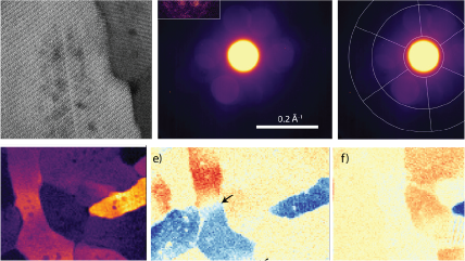
Real-space charge-density imaging with sub-ångstrom resolution by four-dimensional electron microscopy
Gao, W.; Addiego, C.; Wang, H,; Yan, X.; Hou, Y.; Ji, D.; Heikes, C.; Zhang, Y.; Li, L.; Huyan, H.; Blum, T.; Aoki, T.; Nie, Y.; Schlom, D.; Wu, R.; Pan, X.
Influenza A and B virus-like particles produced in mammalian cells are highly immunogenic and induce functional antibodies
Buffin, S.; Peubez, I.; Barrière, F.; Nicolaï, M., -C.; Tapia, T.; Dhir, V.; Forma, E.; Sève, N.; Legastelois, I.
Quantifying inactive lithium in lithium metal batteries
Fang, C.; Li, J.; Zhang, M.; Zhang, Y.; Yang, F.; Lee, J. Z.; Lee, L. M. -H.; Alvarado, J.; Schroeder, M. A.; Yang, Y.; Lu, B.; Williams, N.; Ceja, M.; Yang, L.; Cai, M.; Gu, J.; Xu, K.; Wang, X.; Meng, Y. S.
Direct imaging of tunable crystal surface structures of MOF MIL-101 using high-resolution electron microscopy
Journal of American Chemical Society
Li, X.; Wang, J.; Liu, X.; Liu, L.; Cha, D.; Zheng, X.; Yousef, A. A.; Song, K.; Zhu, Y.; Zhang, D.; Han, Y.
Formation of two-dimensional transition metal oxide nanosheets with nanoparticles as intermediates
Yang, J.; Zeng, Z.; Kang, J.; Betzler, S.; Czarnik, C.; Zhang, X.; Ophus, C.; Yu, C.; Bustillo, K.; Pan, M.; Qiu, J.; Wang, L. -W.; Zheng, H.
Monolayer Ti3C2Tx as an effective co-catalyst for enhanced photocatalytic hydrogen production over TiO2
ACS Applied Energy Material
Su, T.; Hood, Z. D.; Naguib, M.; Bai, L.; Luo, S.; Rouleau, C. M.; Ivanov, I. N.; Ji, H.; Qin, Z.; Wu, Z.
Thermal stability and irradiation response of nanocrystalline CoCrCuFeNi high-entropy alloy
Zhang, Y.; Tunes, M. A.; Crespillo, M. L.; Zhang, F.; Boldman, W. L.; Rack, P. D.; Jiang, L.; Xu, C.; Greaves, G.; Donnelly, S. E.; Wang, L.; Weber, W. J.
The influence of organic modification on the cytotoxicity of clay particles to keratinocytes, hepatocytes and macrophages; an investigation towards the safe use of polymer-clay nanocomposite packaging
Food and Chemical Toxicology
Connolly, M.; Zhang, Y.; Mahri, S.; Brown, D. M.; Ortuño, N.; Jordá-Beneyto, M.; Maciaszek, K.; Stone, V.; Fernandes, T. F.; Johnston, H. J.
2D/2D heterojunction of Ti3C2/g-C3N4 nanosheets for enhanced photocatalytic hydrogen evolution
Su, T.; Hood, Z. D.; Naguib, M.; Bai, L.; Luo, S.; Rouleau, C. M.; Ivanov, I. N.; Ji, H.; Qin, Z.; Wu, Z.
In vitro decidualisation of human endometrial stromal cells is enhanced by seminal fluid extracellular vesicles
Journal of Extracellular Vesicles
Rodriguez-Caro, H.; Dragovic, R.; Shen, M.; Dombi, E.; Mounce, G.; Field, K.; Meadows, J.; Turner, K.; Lunn, D.; Child, T.; Southcombe, J. H.; Granne, I.
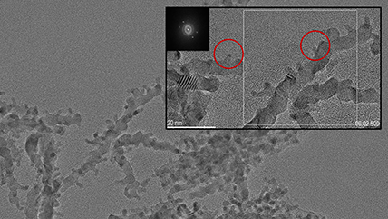
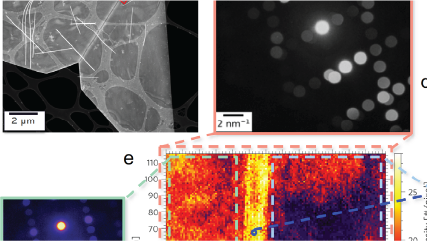
Nanoscale mosaicity revealed in peptide microcrystals by scanning electron nanodiffraction
Gallagher-Jones, M.; Ophus, C.; Bustillo, K. C.; Boyer, D. R.; Panova, O.; Glynn, C.; Zee, C., -T.; Ciston, J.; Mancia, K. C.; Minor, A. M.; Rodriguez, J. A.
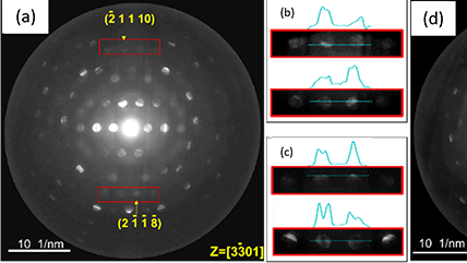
Dynamics of transformation from platinum icosahedral nanoparticles to larger FCC crystal at millisecond time resolution
Gao, W.; Wu, J.; Yoon, A.; Lu, P.; Qi, L.; Wen, J.; Miller, D. J.; Mabon, J. C.; Wilson, W. L.; Yang, H.; Zuo, J. -M.
A high-entropy alloy with hierarchical nanoprecipitates and ultrahigh strength
Fu, Z.; Jiang, L.; Wardini, J. L.; MacDonald, B. E.; Wen, H.; Xiong, W.; Zhang, D.; Zhou, Y.; Rupert, T. J.; Chen, W.; Lavernia, E. J.
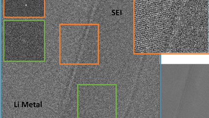
Atomic structure of sensitive battery materials and interfaces revealed by cryo–electron microscopy
Li, Y.; Li.; Y.; Pei, A.; Yan, K.; Sun, Y.; Wu, C. -L; Joubert, L. -M.; Chin, R.; Koh, A. L.; Yu, Y.; Perrino, J.; Butz, B.; Chu, S.; Cui, Y.
Vertical graphene growth on SiO microparticles for stable lithium ion battery anodes
Shi, L.; Pang, C.; Chen, S.; Wang, M.; Wang, K.; Tan, Z.; Gao, P.; Ren, J.; Huang. Y.; Peng, H.; Liu, Z.
Absence of intracellular ion channels TPC1 and 2 leads to mature-onset obesity in male mice, due to impaired lipid availability for thermogenesis in brown adipose tissue
Lear, P. V.; González-Touceda, D.; Couto, B. P.; Viaño, P.; Guymer, V.; Remzova, E.; Tunn, R.; Chalasani, A.; García-Caballero, T.; Hargreaves, I. P.; Tynan, P. W.; Christian, H. C.; Nogueiras, R.; Parrington, J.; Diéguez, C.

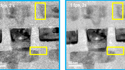
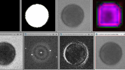
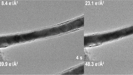
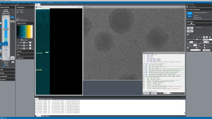
 There are four basic steps in TEM imaging to address incoming electrons:
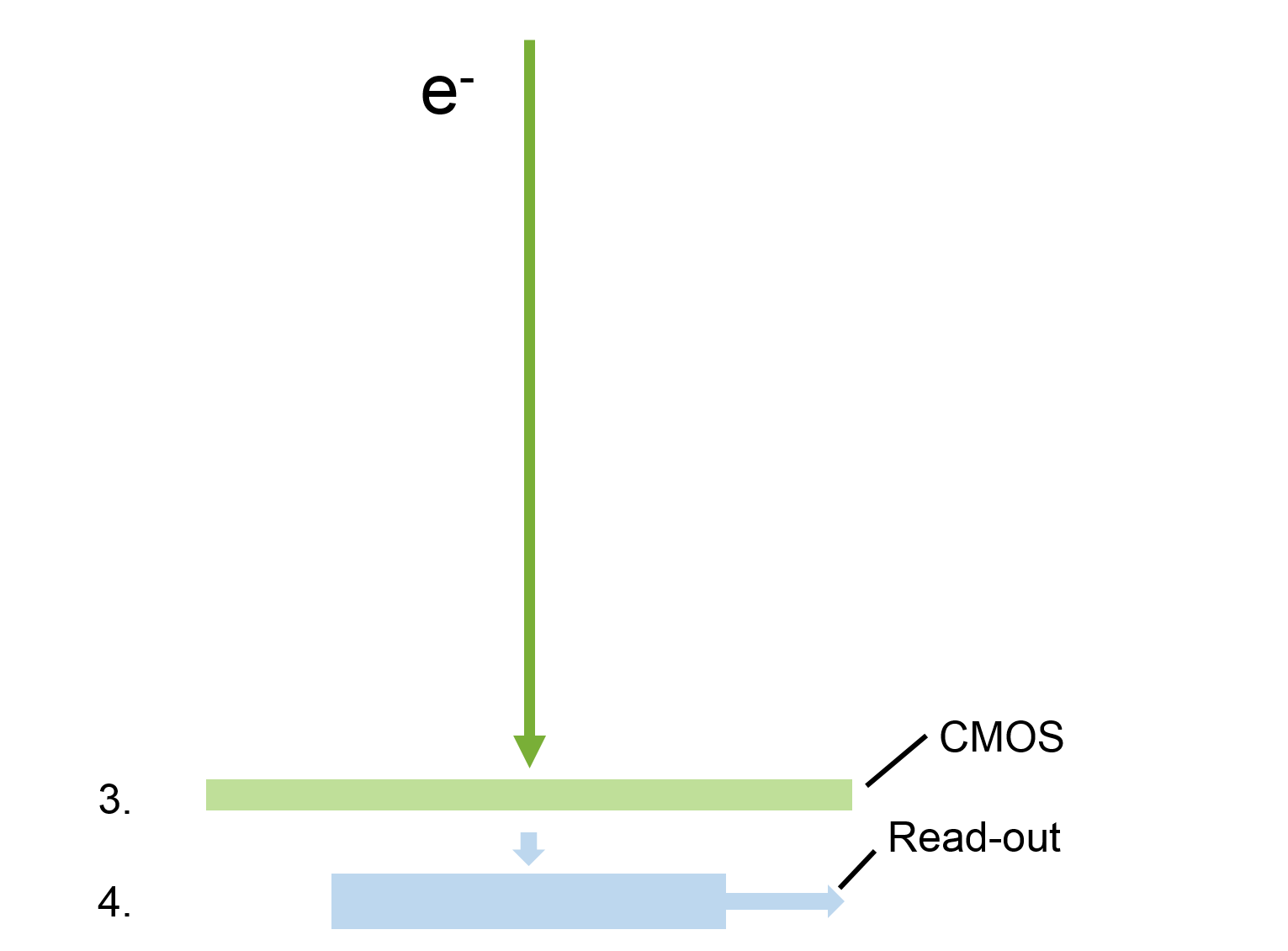
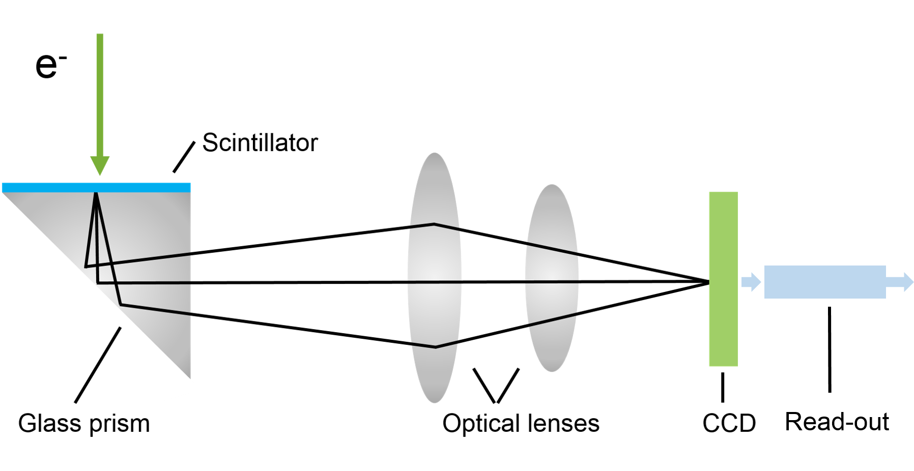
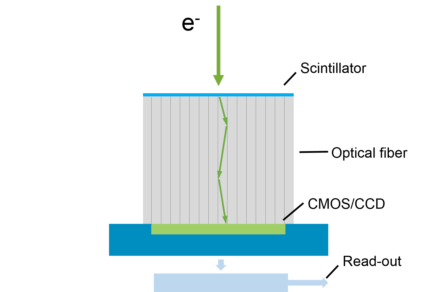
 vs. lens-coupled (right).")