
What is EELS?
Electron energy loss spectroscopy (EELS) represents a sophisticated set of techniques used to probe materials' atomic and chemical properties at a microscopic level. EELS provides invaluable insights into the structure and composition of materials by measuring the change in kinetic energy of electrons after they interact with a specimen.
This technique is pivotal in materials science and nanotechnology, where understanding the atomic structure and chemical properties is crucial. EELS is a versatile technique in that it can determine the type and quantity of atoms present in a material, identify their chemical state, and elucidate optical and acoustic properties of a material. This level of detail is essential for designing new materials with tailored properties for specific applications, from electronics to energy storage.
EELS uses the energy distribution of electrons passing through a thin sample to analyze its content and create images with unique contrast effects. EELS instruments are typically part of a transmission electron microscope (TEM) or a scanning TEM (STEM), both of which use high-energy electrons (60 – 300 kV) to examine the sample. These microscopes require thin, electron-transparent samples since the electrons must transmit through the sample. The electrons can interact with the sample either elastically (no energy exchange) or inelastically, and EELS uses the inelastic interactions to extract information about the sample.
When using EELS on a TEM, detailed analyses of features in the ionization edges can reveal sample information through spectroscopy. Alternatively, the integrated intensity of the edges can be used to create images with contrast related to the elemental distribution of the sample's material, a technique known as energy-filtered transmission electron microscopy (EFTEM). With STEM, you can combine these methods in a technique called spectrum imaging, where spectral information is collected in a spatially resolved manner. This data is used to extract a wealth of information from the sample, including:
- Specimen thickness – Zero-loss peak (ZLP) and total spectrum intensity
- Valence/conduction electron density – Plasmon peaks
- Optical response (complex dielectric function) – Low-loss distribution
- Band structure and interband transitions – Near zero-loss features
- Elemental composition – Core-loss edges
- Bonding and oxidation state (density of unoccupied states) – Energy-loss near edge structure (ELNES)
- Distribution of near neighboring atoms (radial distribution function RDF) – Extended energy loss fine structure (EXELFS)
In essence, EELS is more than just a set of techniques; it's a window into the microscopic world, offering a clearer understanding of materials at the atomic level. This understanding is crucial for advancing technology and developing new materials that meet society's growing demands.
Advantages of EELS
EELS is a powerful technique that takes advantage of the high spatial resolution of (S)TEMs. With STEM-EELS spectrum imaging, it is possible to acquire chemical and structural information from atomically abrupt interfaces simultaneously. Due to the forward scattering of inelastically scattered electrons at lower angles, a large percentage of the signal is collected, resulting in a high signal-to-noise ratio (SNR) in the collected spectra. The strong forward scattering also reduces spurious environmental signals from presenting in the spectra. EELS offers high-energy resolution and a large energy range, allowing for studying a wide variety of material properties, including optical and acoustic properties, oxidation states, and nearest-neighbor distances.
| Capability | Advantage |
|---|---|
| Improves spatial resolution | Results in nearly 100% collection efficiency of inelastic scattering signals and a better SNR |
| Identifies elements within a sample | Identification of spectrum features at distinct energy ranges allows you to discover both the beneficial and detrimental properties of a material |
| Quantifies elements within a sample | Determines the absolute composition of a material so you can distinguish desired from unwanted material phases |
| Locates elements within a sample | Captures the spatial distribution of detected elements with near-atomic resolution to elucidate unique distributions of material at the nanoscale |
| Determines the chemical state and bonding of a sample | Provides insight into the structure and stability of materials |
| Enhances the contrast of your analysis | Allows you to resolve phases and reveal a wealth of information about your material |
Workflow
|
Step 1: Sample preparation Samples are thinned to electron transparency using a method that does not introduce artifacts and minimizes surface damage. For 200 kV electrons, the samples should be less than 100 nm in thickness. The sample must be electrically conductive and rigidly supported by the holder. For STEM experiments, avoiding contamination of the sample, its holder, or the TEM vacuum by hydrocarbons, silicone oils, or similar chemicals is crucial, as this will lead to rapid sample contamination under the beam. |
|
Step 2: Microscope setup and alignment Ensure that the various optical components in the microscope are properly aligned. This will enhance image brightness and minimize image blurring resulting from lens aberrations. |
For EFTEM experiments
|
Step 3: Autotuning Run autotuning for the isochromate to ensure the spectra are focused and to correct image distortions from the prism. |
|
Step 4: Find an area of interest Identify a region of interest in the sample. |
|
Step 5: Set the collection angle Adjust the collection angle by using the objective lens aperture. |
|
Step 6: Acquire elemental maps Choose the elements and acquire the elemental maps. The EFTEM Acquisition pallet in DigitalMicrograph automatically sets the width and range of each window based on the energy-loss edge you selected. |
|
Step 7: Create a composite map Overlay each elemental map to create a composite map. |
For STEM-SI experiments
|
Step 3: Auto ZLP Tune Tune the focus of the zero-loss peak to achieve optimal spectral resolution. Choose the dispersion or spectral magnification during this step. |
|
Step 4: Find an area of interest Identify a region of interest in the sample. |
|
Step 5: Set up and acquire the spectrum image Capture and obtain the spectrum image. |
|
Step 6: Analysis Use the Elemental Quantification pallet in DigitalMicrograph to identify edges in the spectra and build a quantification model. |
|
Step 7: Create a composite map Calculate the elemental concentration for each element to understand its distribution within the sample. |
For more detailed information, visit EELS.info.


DigitalMicrograph, also known as Gatan Microscopy Suite, drives your digital cameras and surrounding components to support key applications including tomography, in-situ, spectrum and diffraction imaging, plus more.

Electron counting for all your EELS, EFTEM, and energy-filtered 4D STEM applications.


A powerful method of obtaining detailed analytic data from a sample on an electron microscope equipped with scanning mode.

Digital beam control and image processing to enhance the photographic quality of your digital images.

Simulation tool to eliminate the guesswork from your EELS and EFTEM compositional mapping experiments.

High-angle annular dark field (HAADF), annular dark field (ADF) plus bright and dark field (BF/DF) detectors for STEM imaging optimized for electron energy loss spectroscopy (EELS).


The most intuitive and easy-to-use energy dispersive spectroscopy (EDS) tool for scanning transmission electron microscope (STEM) applications and in-situ microscopy.

Quantify microstructural changes in materials due to applied mechanical loading.


The EELS and EFTEM systems ideal for multiuser facilities, now with the Stela hybrid-pixel option.

The best-in-class imaging filter for cryo-EM is now available with EELS and EFTEM.


Applications

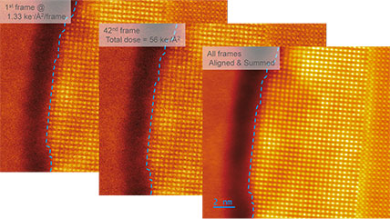
![360 x 50-pixel 2D array dose fractionated EELS SI acquired from SRO/[110] DSO with a 339 µs pixel dwell time.](/sites/default/files/images/2D_Array_Dose_Fractionated_EELS.jpg)

Posters
|
Continuous EELS spectrum imaging of nano-droplet crystallization heterogeneity - EMC 2024 |
|
|