High speed EELS composition analysis, in DualEELS mode, of metal alloy ohmic contacts for the fabrication of III-V MOSFET devices
As the size of III-V devices decreases, ohmic contacts and their performance becomes increasingly significant. In addition to low resistance, these contacts must be reproducible, show good lateral and depth uniformity and be thermally stable. AuGeNi ohmic contacts are widely used as they show a low contact resistivity and are typically compatible with the fabrication of III-V MOSFET devices1. However, they have the drawback of poor uniformity due to the diffusion of the Au into the III-V substrate. This diffusion is dependent on the temperature used during the annealing process after deposition of Au, Ge and Ni. It is clear that the performance of this type of contact will be influenced by both the material present and the degree of roughness at the interface with the III-V substrate; methods to analyze these materials at the sub-nanometer level are required.
To study these interfaces, it is critical to use techniques that can probe a broad range of structural, compositional and chemical properties on real world devices with high throughput. Modern high-angle annular dark field (HAADF) STEM instruments combined with electron energy loss spectroscopy (EELS) spectrum imaging forms a compelling tool. HAADF-STEM provides structural information and qualitative compositional information while EELS provides sensitive quantitative compositional data along with true chemical state data from a range of elements all with sub-nanometer resolution. Since both EELS and HAADF imaging are extremely sensitive techniques, able to probe single atoms in many cases 2,3,4,5, analysis can be performed on sufficiently thin samples to provide high resolution data at a dose low enough to prevent damage and chemical decomposition. The introduction of fast EELS spectrometers, such as the GIF Quantum® 6 and the Enfinium™, has dramatically changed the rate that information can be recorded via EELS spectrum imaging (SI). The detectors in these next generation systems allow EELS chemical maps to be acquired at over 1000 spectra per second allowing the full advantage of the increased brightness available in a probe corrected STEM microscope to be realized. In addition to speed, these detectors support both higher dynamic range and duty cycle acquisition. These advances allow fast EELS spectra with excellent signal-to-noise ratio to be acquired from the high energy region of the EELS spectrum for heavy elements such as Au and Pt with exposure times below 1 ms in some cases. In addition, the electron-optical system present in these EELS spectrometers minimize spectral aberrations up to 5th order allowing large collection angles to be used whilst maintaining the energy resolution. Matching the collection angle to the large STEM probe convergence angles available today is critically important especially for investigating the high energy loss region of the EELS spectrum. Another feature available in the GIF Quantum and the Enfinium is DualEELS™ 7, which allows the near simultaneous acquisition of both the low- and core-loss regions of the EELS spectrum without changing the experimental conditions. Having the low-loss region of the EELS spectrum allows the determination of the absolute number of atoms per unit volume present in the sample, the accurate measurement of chemical shifts due to variations in the local chemistry and the correction for any multiple scattering in the sample allowing the analysis of relatively thick samples. In addition, the optical excitations that are confined in the low-loss region of the EELS spectrum become available for analysis. This is very important for understanding the surface plasmon effects that are present in metallic nanoparticles, for example.
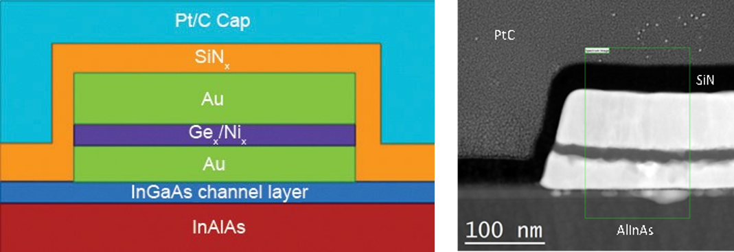
The AuGeNi ohmic contact stack of this study was deposited by electron beam evaporation onto an AlInAs layer previously grown using molecular beam epitaxy (MBE), which is shown schematically in Figure 1. After deposition, the sample underwent a rapid thermal annealing process. Sample was grown using the facilities available at Electrical & Electronics Department at the University of Glasgow, UK. The TEM cross-section was prepared using the FIB situated at the Department of Physics and Astronomy at the University of Glasgow, UK. As a result of the FIB preparation process, this TEM cross-section shows the presence of the electron and ion beam deposited PtC protective layers. A SiN capping layer was also deposited in order to prevent the sample from the damage that might occur during the TEM specimen preparation. Data was acquired using a probe corrected JEOL ARM 200 equipped with Schottky FEG and Enfinium ER EELS system at Arizona State University. EELS SI analysis was carried out in DualEELS mode and the regions of the EELS spectrum from 0 – 2000 eV and from 600 – 2600 eV were simultaneously acquired using exposure times as low as of 0.006 ms and 0.99 ms, respectively. Taking advantage of the fast acquisition available in the Enfinium and the increased probe current, nearly 315,000 spectra (512 x 307 x 2) were acquired in just 420 s with a spectral rate of nearly 800 spectra per second from a wide region of the sample as shown in the annular dark field (ADF) STEM image in Figure 2. The EELS SI data was acquired without any spatial drift correction applied showing the high stability of this microscope installation.
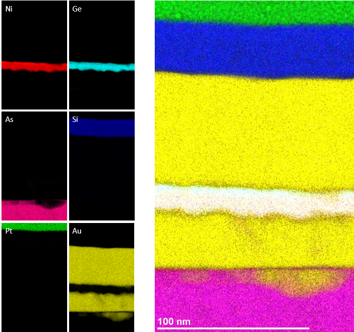
Figures 3A-F show the EELS elemental maps of the sample composition extracted from the Ni L2,3-edges at 855 eV, the Ge L2,3-edges at 1217 eV, the As L2,3-edges at 1323 eV, the Si K-edge at 1839 eV, the Pt M4,5-edges at 2122 eV and the Au M4,5-edges at 2206 eV. Figure 3G shows the EELS colorized elemental map of Ni, Ge, As, Si, Pt and Au. Despite the high energy of some edges involved such as the Si K-edge at 1839 eV and the Pt and Au M4,5-edges at 2122 eV and 2206 eV the contrast shown in those elemental maps is very high and clearly shows where all the elements are located and distributed across the whole investigated region of the sample. It is quite interesting to note that the Ge seems to diffuse more strongly towards the upper Au region whereas the Ni towards the lower. The Au diffuses into the III-V substrate making the interface rough and affecting the electrical performance of the resulting device. The amount of Au diffusing into the substrate depends on the conditions employed during the annealing process and can be quantified using EELS as shown later in this note.
An important aspect of EELS analysis is the EELS signal can be generated at the position of the electron beam and never from secondary scattering fluorescence from other areas of the sample. This is critical when analyzing regions of high atomic number that produce a large flux of Bremsstrahlung x-rays that greatly increase the fluorescence of neighboring atoms. The high energy resolution of the EELS technique allows overlapping edges such as the Pt M4,5–edges at 2122 eV and the Au M4,5–edges at 2206 eV to be easily separated using MLLS fitting routines 8,9.
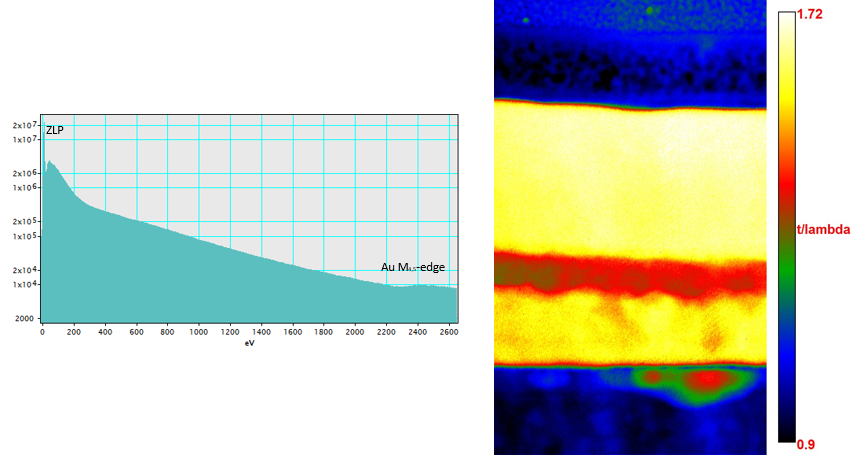
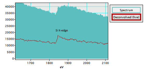
Acquiring the data in DualEELS mode allows the user to have the information from the low-loss region together with the core-loss data. Figure 4 shows an EELS spectrum extracted from the Au region in the sample after splicing the two datasets at high and low energy. The dynamic range has been clearly increased and the resultant EELS spectrum extends from 0 – 2600 eV. Given the presence of the low-loss region in the same dataset under identical experimental conditions provides information on the thickness which can be easily measured as shown in Figure 5. The sample seems quite thick as the thickness ranges from 0.8 – 1.72 relative to the mean free path (l). However having the low-loss in the same dataset under the same experimental conditions allows the plural scattering to be deconvolved recovering the single scattering distribution. In this way, the effects of plural scattering, which are bigger as the thickness increases, can be accounted and the EELS spectra can be deconvolved to single scattering distribution. Figure 6 shows the EELS spectrum of the Si K-edge at 1839 eV extracted from the SiN capping layer region before and after deconvolution. The contribution of the plural scattering is quite strong in this case. However, after deconvolution, it is possible to see that the shape of the extracted Si K-edge belongs to SiN.
Another advantage of acquiring data in DualEELS mode is that the compositional analysis becomes more accurate, due to the fact that core-loss signals can be readily normalized with the low-loss allowing non-compositional intensity artifacts in the elemental map to be completely removed. In addition, measuring the absolute composition (atoms per unit area rather than simple composition ratios) requires the low-loss contribution to be included as per the following equation:
Where N is the number of atoms per unit area of the specimen under the beam that contribute to the k-edge; Ik is the integral for an edge k at a given integration window Δ and collection angle β after removal of plural scattering and spectral background; σk is the computed scattering cross-section for edge k at a given Δ and β (typically generated from Hartree-Slater atomic cross sections automatically in DigitalMicrograph® software); I0 is the zero-loss integral at a given β10. The absolute number of atoms per unit volume can be easily obtained by dividing N for the absolute thickness which can be accessed from the low-loss portion of the EELS spectrum.
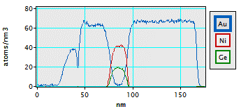
Figure 7 shows the absolute number of atoms of Au, Ge and Ni extracted from the metal ohmic contact region. The measured value of 66 Au-atoms/nm3 agrees well with the typical value of 59 atoms/nm3 for bulk gold. In this case, for the Au, the accuracy of the measurements is within 7 atoms/nm3. In general, the error in the compositional analysis using EELS is due to a combination of factors such as the cross-section, the background extraction and the thickness. The error in the cross-section measurement depends on the cross-section type. For instance, K-edges show the highest accuracy whereas the M-edges the lowest. Thus, in the case of this study the biggest error is expected for the Au M4,5-edges.
We have shown that high speed atomic EELS elemental maps with high contrast and high signal-to-noise ratios can be acquired routinely from high-energy edges. In addition, using the DualEELS capability, which is available in both the GIF Quantum and the Enfinium systems, it is possible to record simultaneously two different regions of the EELS spectrum under the same experimental conditions. Some applications and advantages of the acquisition in DualEELS mode are reported in this note.
References:
- R.J.W. Hill, D.A.J. Moran, X. Li, H. Zhou, D. Macintyre, S. Thoms, A. Asenov, P. Zurcher, J. Abrokwah, R. Droopad, M. Passlack and I.G. Thayne, IEEE Electron Devices Letters, 28, 2007, 12.
- Krivanek O. et al., Nature 464, 571 – 574, 2010.
- Suenaga K. et al., Nature Chem. 1, 415 – 418, 2009.
- Leapman R.D., J. Microsc., 210, 5 – 15, 2003.
- Robb P.D., Finnie M., Longo P. and Craven A.J., Ultramicroscopy, 114, 11 – 19, 2012.
- A.J. Gubbens, M. Barfels, C. Trevor, R. D. Twesten, P. J. Thomas, N. Menon, B. Kraus, C. Mao and B. McGinn, Ultramicroscopy, 110, 962 – 970, 2010.
- J. Scott, P.J. Thomas, M. Mackenzie, S. Mcfadzean, A.J. Craven and W.A.P. Nicholson, Ultramicroscopy, 108, 1586 – 1594, 2008.
- P.J. Thomas, Gatan Inc., Knowhow 14 December 2006.
- P. Longo, Gatan Inc, Applications note September 2011.
- Egerton, “Electron Energy-Loss Spectroscopy in the Electron Microscopy 3rd Edition”, Springer, New York 2011.