半導体材料とデバイス
共通の課題
マイクロエレクトロニクス業界で開発されている先端材料は、デバイスの微細化や新たな三次元構造の開発に望ましい数多くの独自の特性を備えています。材料の具体的な特性としては、極めて高い強度、柔軟性、光透過性、熱伝導性などがあります。研究者たちがこれらの材料の製造と特性評価に膨大な労力を注ぐ一方で、これらの材料の新製品への投入とその後の製造プロセスが引き続き課題となっています。通常、これらの課題は、製造を進める上で必須プロセスの精度とデバイスの生産性に影響を与えます。これらの課題に先手を打ちハードルを下げるには、以下の情報が役立ちます。
- 材料またはデバイスの原子組成
- トランジスター素子の制御に与える影響
- 化学特性
- 材料特性を明らかにするための分析の手法確立と容易さ
革新的な手法
半導体材料やデバイスの特性を的確に評価し、理解するには、まず最初に、材料界面を識別できるように各試料が高品質であることと、必要に応じて環境刺激下で処理できるように各試料が適切に管理されていることが重要です。試料を作製したら、デバイスの性能を向上させるため、材料の複雑さと欠陥をより深く理解するためにいくつかの手法を利用できます。
原子分解能の化学および組成分析。
|
ナノメートルレベルの分解能で像内の元素と化学物質を強調しマッピングを行い定量化するイメージング手法の1つ。
|
EELSデータの空間分布を生成するための体系的な方法。
|
材料の成長、素子の超微細構造と不具合を理解するのに役立つ、権威ある賞を受賞した高分解能イメージングツール。
|
成長過程、化学反応と酸化、照射効果、機械特性、磁気特性、強誘電特性をリアルタイムで観察。
|
独自のSEM、TEM、またはSTEMアプリケーション用に試料を切削、エッチング、研磨、および凍結するための高性能ツール。
|
試料の元素または化学特性を解明するのに役立つ。
|
材料の結晶方位や組織を調べるのに役立つ。
|
関連するアプリケーションの詳細については、「発光材料および発光デバイス」または「電池およびエネルギー貯蔵技術」をご覧ください。
結果の活用
組成分析
AuGeNi オーミック接点は、接点の抵抗が小さく、一般的にIII-V MOSFET素子の製造に適しているため、広く使用されています。しかし、III-V回路基板にAuが拡散するため、均一性に劣るという短所があります。この拡散は、Au、Ge、Niのデポジション後の焼きなまし処理時の温度に依存します。EELS手法やEFTEM手法を使用すると、III-V回路基板との接合部分に存在する物質と接合部分の粗さが素子の性能にどのように影響するのかを調べることができます。試料はグラスゴー大学様、顕微鏡はアリゾナ州立大学(アリゾナ州、テンピ)のRay Carpente教授のご厚意によるものです。実験を行う際の顕微鏡の設定は、Jeol USA(現在のASU)のToshiro Aoki博士にご協力いただきました。
トランジスター制御の理解
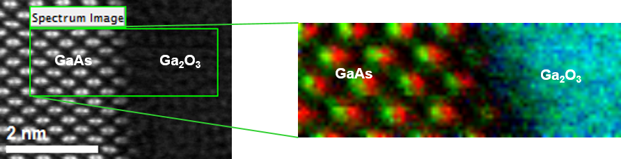
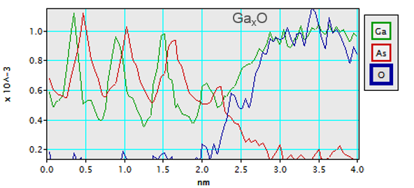
II-V半導体上の酸化物の原子EELS分析を実施すると、As、O、Gaの強度ラインプロファイルを抽出できます。この例では、GaAsのダンベル構造を明確に解像できるだけでなく(カラーマップの左側)、GaとAsの原子列も可視化できます。界面領域では、Ga2O単分子層の存在も確認することができ、電子素子のオン/オフの切り替えを可能にするフェルミ準位がピンニングされていない原因になっていることがわかります。左上の画像:環状暗視野(ADF) STEM像。右上の画像:EELSカラーマップ。Ga:緑色、As:赤色、O:青色。試料はグラスゴー大学様、電子顕微鏡はフロリダ州立大学(フロリダ州、タラハシー)のYan Xin博士のご厚意によるものです。実験を行う際の顕微鏡の設定は、Jeol USA(現在のASU)のToshiro Aoki博士にご協力いただきました。
化学分析
分子の状態、密度、原子分布を理解することは、半導体素子の化学的状態を正確に特性評価する上で重要です。下の元素マップのスペクトル画像は、バンド構造内の化学的状態とシフトをより深く理解するために、複数の手法(エネルギー損失吸収端微細構造(ELNES)、エネルギー損失微細構造(EXELFS)、原子固有の動径分布関数(RDF))をどのように組み合わせることができるのかを示しています。
分析手法の確立と容易さ
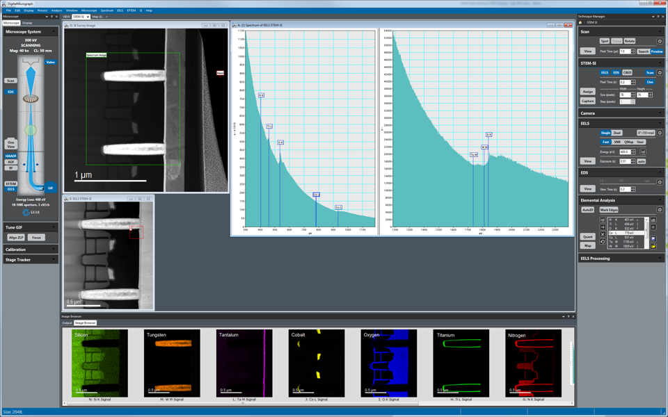
Gatan Microscopy Suite® (GMS)を使用すると、再現可能な方法で簡単に半導体を分析することができます。GMSは、シンプルになったユーザーインターフェイスと実験重視のワークフローを備えた、最先端の電子顕微鏡法ソフトウェアの完全改訂版です。このソフトウェアは、完全にインタラクティブなユーザーインターフェイスと電子顕微鏡へのアクセス、最新のデータ処理と手法に基づくワークフロー、ユーザーフレンドリーなEELSおよびEDSによる定量化機能を備え、結果を得るためのプロセスではなく結果そのものに集中することができます。
パブリケーション
-
Advanced Science2022
-
Large bandgap insulating superior clay nanosheets
MRS Bulletin2022Pacakova, B.; Vullum, P. E.; Kirch, A.; Breu, J.; Miranda, C. R.; Fossum, J. O. -
High-density switchable skyrmion-like polar nanodomains integrated on silicon
Nature2022Han, L.; Addiego, C.; Prokhorenko, S.; Wang, M.; Fu, H.; Nahas, Y.; Yan, X.; Cai, S.; Wei, T.; Fang, Y.; Liu, H.; Ji, D.; Guo, W.; Gu, Z.; Yang, Y.; Wang, P.; Bellaiche, L.; Chen, Y.; Wu, D.; Nie, Y.; Pan, X. -
Observation of ferroelastic and ferroelectric domains in AgNbO3 single crystal
Chinese Physics Letters2022Zhao, W.; Fu, Z.; Deng, J.; Li, S.; Han, Y.; Li, M. -R.; Wang, X.; Hong, J.; -
Spinterface induced modification in magnetic properties in Co40F e40B20/fullerene bilayers
arXiv2021Sharangi, P.; Pandey, E.; Mohanty,S.; Nayak, S.; Bedanta, S. -
Laser-induced graphenization of PDMS as flexible electrode for microsupercapacitors
Advanced Materials Interfaces2021Zaccagnini, P.; Ballin, C.; Fontana, M.; Parmeggiani, M.; Bianco, S.; Stassi, S.; Pedico, A.; Ferrero, S.; Lamberti, A. -
Chemical vapor deposition of highly conjugated, transparent boron carbon nitride thin films
Advanced Science2021Giusto, P.; Cruz, D.; Heil, T.; Tarakina, N.; Patrini, M.; Antonietti, M. -
Electronically coupled 2D polymer/MoS2 heterostructures
Journal of American Chemical Society2020Balch, H. B., Evans, A. M., Dasari, R. R., Li, H., Li, R., Thomas, S., Wang, Q., Bisbey, R. P., Slicker, K., Castano, I., Xun, S., Jiang, L., Zhu, C., Gianneschi, N., Ralph, D. C., Brédas, J-L., Marder, S. R., Dichtel, W. R., Wang, F. -
Electric-field control of chirality
arXiv2021Behera, P.; May, M. A.; Gómez-Ortiz, F.; Susarla, S.; Das, S.; Nelson, C. T.; Caretta, L.; Hsu, S. -L.; McCarter, M. R., Savitzky, B. H.; Barnard, E. S.; Raja, A.; Hong, Z.; García-Fernandez, P.; Lovesey, S. W.; van der Laan, G.; Ophus, C.; Martin, L. W.; Junquera, J.; Raschke, M. A.; Ramesh, R. -
Spatial mapping of electrostatics and dynamics across 2D heterostructures
Condensed Matter2020Murthy, A. A.; Stanev, T. K.; Ribet, S. M.; Liu, P.; Watanabe, K.; Taniguchi, T.; Stern, N. P.; dos Reis, R.; Dravid, V. P. -
In situ TEM study of crystallization and chemical changes in an oxidized uncapped Ge2Sb2Te5 film
Journal of Applied Physics2020Singh, M. K.; Ghosh, C.; Miller, B.; Kotula, P. G.; Tripathi, S.; Watt, J.; Bakan, G.; Silva, H.; Carter, C. B. -
Plasma profiling time-of-flight mass spectrometry for fast elemental analysis of semiconductor structures with depth resolution in the nanometer range
arXiv.org2019Spende, H.; Margenfeld, C.; Meyer, T.; Clavero, I. M.; Bremers, H.; Hangleiter, A.; Seibt, M.; Waag, A.; Bakin, A. -
Large piezoelectric coefficient with enhanced thermal stability in Nb5+-doped Ba0.85Ca0.15Zr0.1Ti0.9O3 ceramics
Ceramics International2019He, L.; Ji, Y.; Ren, S.; Zhao, L.; Luo, H.; Liu, C.; Hao, Y.; Zhang, L.; Zhang, L.; Ren, X. -
Correlation of threading dislocations with the electron concentration and mobility in InN heteroepitaxial layers grown by MBE
ECS Journal of Solid State Science and Technology2019Adikimenakis, A.; Chatzopoulou, P.; Dimitrakopulos, G. P.; Kehagias, Th.; Tsagaraki, K.; Androulidaki, M.; Doundoulakis, G.; Kuzmik, J.; Georgakilas, A. -
Effects of substrate and post‐deposition annealing on structural and optical properties of (ZnO)1−x(GaN)x films
Basic Solid State Physics2019Olsen, V. S.; Bazioti, C.; Baldissera, G.; Azarov, A.; Prytz, Ø.; Persson, C.; Svensson, B. G.; Kuznetsov, A. Y.; Vines, L. -
In situ observations of reversible vacancy ordering process in van der Waals bonded Ge-Sb-Te thin films and GeTe-Sb2Te3 superlattices
Nanoscale2019Lotnyk, A.; Dankwort, T.; Hilmi, I.; Kienle, L.; Rauschenbach, B. -
Local electrochemical properties of fusion boundary region in SA508-309L/308L overlay welded joint
Corrosion Science2019Lai, Z.; Bi, P.; Wen, L.; Xue, Y.; Jin, Y. -
Fermi level shift in carbon nanotubes by dye confinement
Carbon2019Almadoria, Y.; Delport, G.; Chambard, R.;Orcin-Chaix, L.; Selvati, A. C.; Izard, N.; Belhboub, A.; Aznar, R.; Jousselme, B.; Campidelli, S.; Hermet, P.; Le Parca, R.; Saito, T.; Sato, Y.; Suenaga, K.; Puech, P.; Lauret, J. S.; Cassabois, G.; Bantignies, J. -L.; Alvarez, L. -
Chiral twisted van der Waals nanowires
Nature Letters2019Sutter, P.; Wimer, S.; Sutter, E. -
Simple synthesis of highly uniform bilayer-carbon nanocages
Carbon 20172017Ziolkowska, D. A.; Jangam, J. S. Dilip; Rudakov, G.; Paronyan, T.; Akhtar, M.; Sumanasekera, G.; Jasinski, J. B. -
Nanoscale engineering in VO2 nanowires via direct electron writing process
Nano Letters2017Zhang, Z.; Guo, H.; Ding, W.; Zhang, B.; Lu, Y.; Ke, X.; Liu, W.; Chen, F.; Sui, M. -
High temperature-stability of (Pb 0.9 La 0.1 )(Zr 0.65 Ti 0.35 )O 3 ceramic for energy-storage applications at finite electric field strength
Scripta Materialia2017Gao, J.; Liu, Y.; Wang, Y.; Wang, D. -
Local nanoscale strain mapping of a metallic glass during in situ testing
Applied Physics Letters2018Gammer, C.; Ophus, C.; Pekin, T. C.; Eckert, J.; Minor, A. M. -
Correlation between electrical transport and nanoscale strain in InAs/In0.6Ga0.4As core–shell nanowires
Nano Letters2018Zeng, L.; Gammer, C.; Ozdol, B.; Nordqvist, T.; Nygård, J.; Krogstrup, P.; Minor, A. M.; Jäger, W.; Olsson, E. -
Probing light atoms at sub-nanometer resolution: Realization of scanning transmission electron microscope holography
Cornell University Library2018Yasin, F. S.; Harvey, T. R.; Chess, J. J.; Pierce, J. S.; Ophus, C.; Ercius, P.; McMorran, B. J. -
Structure and chemistry of epitaxial ceria thin films on yttria-stabilized zirconia substrates, studied by high resolution electron microscopy
Ultramicroscopy2017Sinclair, R.; Lee, S. C.; Shi, Y.; Chueh, W. C. -
Unravelling surface and interfacial structures of a metal–organic framework by transmission electron microscopy
Nature Materials2017Zhu, Y.; Ciston, J.; Zheng, B.; Miao, X.; Czarnik, C.; Pan, Y.; Sougrat, R.; Lai, Z.; Hsiung, C. -E.; Yao, K.; Pinnau, I.; Pan, M.; Han, Y. -
Electron-beam induced transformations of layered tin dichalcogenides
Nano Letters2016Sutter, E.; Huang, Y.; H.-P. Komsa, H. -P.; Ghorbani-Asl, M.; Krasheninnikov, A. V.; Sutter, P. -
The biosynthesis of infrared-emitting quantum dots in allium fistulosum
Scientific Reports2016Green, M.; Haigh, S. J.; Lewis, E. A.; Sandiford, L.; Burkitt-Gray, M.; Fleck, R.; Vizcay-Barrena, G.; Jensen, L.; Mirzai, H.; Curry, R. J.; Dailey, L. -A. -
Self-sensitized photocatalytic degradation of colorless organic pollutants attached to rutile nanorods – Experimental and theoretical DFT+D studies
Journal of Physical Chemistry C2016Qi, K.; Zasada, F.; Piskorz, W.; Indyka, P.; Gryboś, J.; Trochowski, M.; Buchalska, M.; Kobielusz, M.; Macyk, W.; Sojka, Z. -
Cathodoluminescence and electron microscopy of red quantum dots used for display applications
Journal of the Society for Information Display2015Fern, G. R.; Silver, J.; Coe-Sullivan, S. -
Electron energy loss spectroscopy and localized cathodoluminescence characterization of GaN quantum discs
Microscopy and Microanalysis2014Williams, R. E. A.; Carnevale, S. D.; Kent, T. F.; Stowe, D. J.; Myers, R. C.; McComb, D. W. -
Investigating the origin of luminescence in zinc oxide nanostructures with STEM-cathodoluminescence
Microscopy and Microanalysis2015White, E. R.; Howkins, A.; Williams, C. K.; Shaffer, M. S. P. -
Nanoscale optical and electrical characterizations of ZnO nanostructures by near-field microscopy
SPIE Proceedings2016Teherani, F. H.; Look, D. C.; Rogers, D. J. -
Nanocathodoluminescence reveals mitigation of the Stark shift in InGaN quantum wells by Si doping
Nano Letters2015Griffiths, J. T.; Zhang, S.; Rouet-Leduc, B.; Fu, W. Y.; Bao, A.; Zhu, D.; Wallis, D. J.; Howkins, A.; Boyd, I.; Stowe, D.; Kappers, M. J.; Humphreys, C. J.; Oliver, R. A. -
Microstructure and tribological properties of MoS2 + Zr composite coatings in high humidity environment
Applied Surface Science2016Ye, M.; Zhang, G.; Ba, Y.; Wang, T.; Wang, X.; Liu, Z. -
Atomic level 1D structural modulations at the negatively charged domain walls in BiFeO3 films
Advanced Materials Interfaces2015Wang, W. -Y.; Tang, Y. -L.; Zhu, Y. -L.; Xu, Y. -B.; Liu, Y.; Wang, Y. -J.; Jagadeesh, S.; Ma, X. -L. -
Role of oxygen functional group in graphene oxide for reversible room-temperature NO2 sensing
Carbon2015Choi, Y. R.; Yoon, Y. -G.; Choi, K. S.; Kang, J. H.; Shim, Y. -S.; Kim, Y. H.; Chang, H. J.; Lee, J. -H.; Park, C. R.; Kim, S. Y.; Jang, H. W. -
Real-time observation of morphological transformations in II–VI semiconducting nanobelts via environmental transmission electron microscopy
Nano Letters2015Agarwal, R.; Zakharov, D. N.; Krook, N. M.; Liu, W.; Berger, J. S.; Stach, E. A.; Agarwal, R. -
Interface-induced nonswitchable domains in ferroelectric thin films
Nature Communications2014Han, M-G.; Marshall, M. S. J.; Wu, L.; Schofield, M. A.; Aoki, T.; Twesten, R.; Hoffman, J.; Walker, F. J.; Ahn, C. H.; Zhu, Y. -
Thermal, optical, and electrical characterization of thin film coated RTV 655 bilayer system
Journal of Applied Polymer Science2014Sabri, F.; King, D. S.; Lokesh, A.; Hatch, C. J.; Duran, R. A. -
Self-catalytic growth of β-Ga2O3 nanostructures by chemical vapor deposition
Advanced Engineering Materials2014Kumar, S.; Tessarek, C.; Sarau, G.; Christiansen, S.; Singh, R. -
Selective patterning of gold surfaces by core/shell, semisoft hybrid nanoparticles
Small2014Moraes, J.; Ohno, K.; Maschmeyer, T.; Perrier, S. -
Atomic scale real-space mapping of holes in YBa2Cu3O6+δ
Nature Communications2013Gauquelin, N.; Hawthorn, D. G.; Sawatzky, G. A.; Liang, R. X.; Bonn, D. A.; Hardy, W. N.; Botton, G. A. -
Understanding and controlling low-temperature aging of nanocrystalline materials
Sandia Report2013Battaile, C. C.; Boyce, B. L.; Brons, J. G.; Foiles, S. M.; Hattar, K. A.; Holm, E. A; Padilla, H. A.; Sharon, J. A.; Thompson, G. B. -
Orienting semiconducting nanocrystals on nanostructured polycarbonate substrates: Impact of substrate temperature on polymorphism and in-plane orientation
Macromolecules2011Vergnat, C.; Landais, V.; Legrand, J. F.; Brinkmann, M. -
Real-time observation of impurity diffusion in silicon nanowires
Nano Letters2011Holmberg, V. C.; Collier, K. A.; Korgel, B. A. -
Gold catalyzed nickel disilicide formation: A new solid–liquid-solid phase growth mechanism
Nano Letters2013Tang, W.; Picraux, S. T.; Huang, J. H.; Liu, X.; Tu, K. N.; Dayeh, S. A. -
Hand book of nanoscopy
Wiley-VCH2012Van Tendeloo, G.; Van Dyck, D.; Pennycook, S. J. -
Elucidating elementary processes at Cu/ZnO interfaces: A microscopical approach
Physica Status Solidi2013Zychma, A.; Wansing, R.; Schott, V.; Köhler, U.; Wöll, C.; Muhler, M.; Birkner, A. -
Strain measurement in semiconductor heterostructures by scanning transmission electron microscopy
Microscopy and Microanalysis2012Müller, K.; Rosenauer, A.; Schowalter, M.; Zweck, J.; Fritz, R.; Volz, K. -
Influence of a single grain boundary on domain wall motion in ferroelectrics
Advanced Functional Materials2014Marincel, D. M.; Zhang, H.; Kumar, A.; Jesse, S.; Kalinin, S. V.; Rainforth, W. M.; Reaney, I. M.; Randall, C. A.; Trolier-McKinstry, S. -
Ga ordering and electrical conductivity in nanotwin and superlattice-structured Ga-doped ZnO
Crystal Growth and Design2012Yoon, S. W.; Seo, J. H.; Seong, T. Y.; Yu, T. H.; You, Y. H.; Lee, K. B.; Kwon, H.; Ahn, J. P. -
Development of a focused ion beam (FIB) technique to minimize X-ray fluorescence during energy dispersive X-ray spectroscopy (EDS) of FIB specimens in the transmission electron microscope (TEM)
Ultramicroscopy1999Longo, D. M.; Howe, J. M.; Johnson, W. C. -
Electronic structure of supelattice and twin in Ga doped ZnO measured by monochromated EELS
Microscopy and Microanalysis2011Chang, H.; Yoon, S.; Seong, T.; Yu, T.; Yuo, Y.; Ahn, J. -
Orientation dependence of shock-induced twinning and substructures in a copper bicrystal
Acta Materialia2010Cao, F.; Beyerlein, I. J.; Addessio, F. L.; Sencer, B. H.; Trujillo, C. P.; Cerreta, E. K.; Gray III, G. T. -
Single crystalline La0.7Sr0.3MnO3 molecular sieve nanowires with high temperature ferromagnetism
Journal of American Chemical Society2011Carretero-Genevrier, A.; Gázquez, J.; Idrobo, J. C.; Oró, J.; Arbiol, J.; Varela, M.; Ferain, E.; Rodríguez-Carvajal, J.; Puig, T.; Mestres, N.; Obradors, X. -
Thermally robust anion-chain order in oxynitride perovskites
Chemistry of Materials2013Clark, L.; Oró-Solé, J.; Knight, K. S.; Fuertes, A.; Attfield, J. P. -
Direct monolithic integration of vertical single crystalline octahedral molecular sieve nanowires on silicon
Chemistry of Materials2014Carretero-Genevrier, A.; Oro-Sole, J.; Gazquez, J.; Magén, C.; Miranda, L.; Puig, T.; Obradors, X.; Ferain, E.; Sanchez, C.; Rodriguez-Carvajal, J.; Mestres, N. -
Electronic tuning of two metals and colossal magnetoresistances in EuWO1+xN2−x perovskites
Journal American Chemical Society2010Yang, M.; Oró-Solé, J.; Kusmartseva, A.; Fuertes, A.; Attfield, J. P. -
Interactions of gold nanoparticles with the interior of hollow graphitized carbon nanofibers
Small2012La Torre, A.; Fay, M. W.; Rance, G. A.; Gimenez-Lopez, M. d. C.; Solomonsz, W. A.; Brown, P. D.; Khlobystov, A. N. -
Dislocation-filtering AlInSb buffer layers for InSb quantum wells—Analysis by high-tilt bright-field and dark-field TEM
Physica E: Low-dimensional Systems and Nanostructures2010Mishima, T. D.; Edirisooriya, M.; Santos, M. B. -
Micro-twin defects in InSb/AlInSb layers grown on (001) GaAs∼ Application of the-directional TEM analysis∼
Physics Procedia2010Mishima, T. D.; Santos, M. B. -
Aberration-corrected and energy filtered precession electron diffraction
Crystalline Materials2012Eggeman, A. S.; Barnard, J. S.; Midgley, P. A. -
Combining HRTEM–EELS nano-analysis with capacitance–voltage measurements to evaluate high-κ thin films deposited on Si and Ge as candidate for future gate dielectrics
Microelectronic Engineering2011Schamm-Chardon, S.; Coulon, P.E.; Lamagna, L.; Wiemer, C.; Baldovino, S.; Fanciulli, M. -
Complete composition tunability of InGaN nanowires using a combinatorial approach
Nature Materials2007Kuykendall, T.; Ulrich, P.; Aloni, S.; Yang, P. -
Arsenic dopant mapping in state-of-the-art semiconductor devices using electron energy-loss spectroscopy
Micron2009Servanton, G.; Pantel, R. -
Cross-sectional transmission electron microscopy of GaAs quantum dots fabricated by filling of droplet-etched nanoholes
Journal of Crystal Growth2011Nemcsics, Á.; Heyn, Ch.; Tóth, L.; Dobos, L.; Stemmann, A.; Hansen, W. -
Aberration-corrected transmission electron microscopy analyses of GaAs/Si interfaces in wafer-bonded multi-junction solar cells
Ultramicroscopy2013Häussler, D.; Houben, L.; Essig, S.; Kurttepeli, M.; Dimroth, F.; Dunin-Borkowski, R. E. -
Optical properties and bandgaps from low loss EELS: Pitfalls and solutions
Micron2008Stöger-Pollach, M. -
Four-dimensional STEM-EELS: Enabling nano-scale chemical tomography
Ultramicroscopy2009Jarausch, K.; Thomas, P.; Leonard, D. N.; Twesten, R.; Booth, C. R. -
Nanoscale EELS analysis of dielectric function and bandgap properties in GaN and related materials
Micron2000Borckt, G.; Lakner, H.