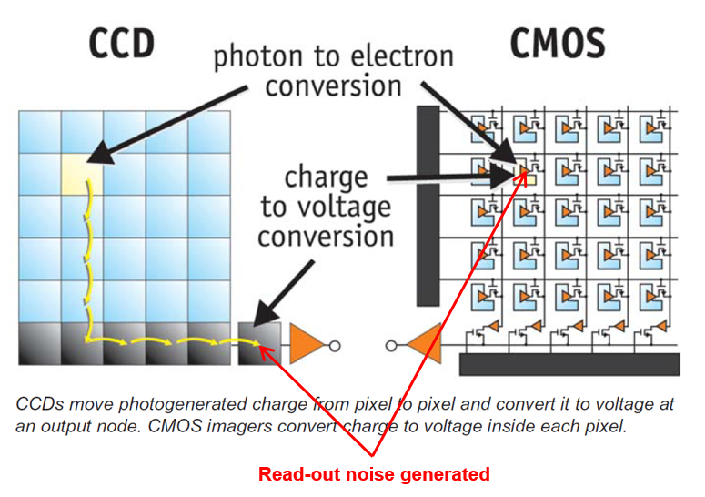
CCD vs. CMOS
Binning Read-out Sensors Anti-blooming
Binning: Signal-to-noise ratio, dynamic range, and speed benefits
In the case of CCD sensors, binning can significantly improve the output signal-to-noise ratio (SNR) when you combine signal in adjacent pixels, then apply a single read-out (noise) against the summed signal. The diagram below demonstrates how this summing applies for bin x2, but similar scaling can happen for any binning mode. In general, the binning is done in a square pattern (e.g., 2 x 2, 4 x 4, 8 x 8 …), but there may be applications where it is advantageous to bin in only one direction.
| 1x (no) Binning | 2x Binning | |
|---|---|---|
| Collect signal in each pixel |  |
 |
| Transfer charge to read-out register | 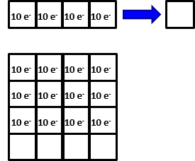 |
 |
| Convert to voltage, amplification, and read-out |  |
 |
In the case of CMOS devices, the charge-to-voltage conversion is done in each pixel, therefore the read-out noise is applied per pixel: Instead of N-fold benefit it only becomes N1/2 (see illustration below).
Binning reduces resolution (loss of pixels), however speed does not scale proportionally to a CCD since you need to address each pixel individually. Depending on the specific CMOS design, it is possible to perform localized charge binning on adjacent pixels if the correct transistor architecture implemented and selected on the sensor design.
Sensors: Full frame vs. interline (CCD)
Full frame: 100% pixel coverage, captures all incoming light (e.g., signal)
In the case of full frame CCD sensors, the entire sensor area is dedicated to photosensitive receptors. The electron beam must be blanked during read-out, plus you should note that a very slow shutter speed may introduce blur into the images.
- Pros
- Best/most information for most sensitive applications and signal-to-noise
- Full fill factor
- Can contain large pixels and highest full-well capacity
- Cons
- Microscope shuttering speeds may limit higher frame rates due to smaller duty cycles at fastest frames per second (fps)
- Slow shutters may introduce blur into images
Interline: 100% in time with masked area used to read-out charge without mechanical shutter
After you transfer the charge for each pixel to a masked area (non photo-sensitive), the charge for each pixel is read-out while you capture the next frame’s image. Keep in mind that the maximum frame rate is the time it takes to fully read-out the sensor, but that there is 100% duty cycle as you are always collecting information.
- Pros: Fast fps since read-out can be done without microscope shuttering; always collecting signal
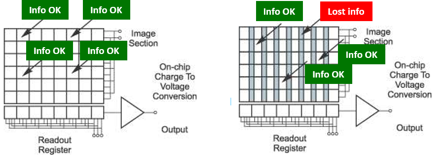
- Cons: Some loss in detection signal area due to the read-out columns; you can mitigate by point spread function (PSF) of signal across full pixel size
Conclusion: There is not a single sensor preference to address all applications. The best sensor will be dependent upon what application is being targeted in terms of speed, fill factor, noise requirements, beam conditions, etc.
Anti-blooming
Blooming (vertical streaking) is caused by excess charge spilling over into a vertical transfer register from a given pixel.
 CMOS sensors are inherently more immune to blooming because the charge converts to voltage in each pixel before read-out; there is no charge transfer register to spill over into
- Many CCD cameras have anti-blooming design features incorporated to allow charge to dissipate without affecting neighbor pixels; particularly important for diffraction applications