Antiferroelectric PbSnO3 epitaxial thin films
Advanced Science
2022
Emerging materials for the microelectronics industry possess a number of unique properties that make them particularly desirable to shrink device geometries and develop novel 3D architectures. Specific material properties include their extreme strength, flexibility, optical transparency and thermal conductivity. While researchers focus an enormous amount of effort on the fabrication and characterization of these materials, integration of these materials into new products and their subsequent industrialization continues to be a challenge. These challenges commonly affect the precision of a required process and repeatable yield of devices as they are industrialized. Useful information to prevent or mitigate these challenges include:
To adequately characterize and understand semiconductor materials or devices, you must first ensure each specimen is of the highest quality to resolve the material interface and properly controlled so you manipulate it, when necessary, under environmental stimuli. Once prepared, several techniques are available to better understand material complexities and failures to improve device performance.
|
Atomic resolution chemical and compositional analysis.
|
Family of imaging techniques to enhance, map and quantify elements and chemicals in an image with nanometer resolution.
|
|
Systematic method to generate a spatially resolved distribution of EELS data.
|
Award winning, high resolution imaging tools help you to understand material growth, devices ultrastructure and failures.
|
|
Real-time observation of growth processes, chemical reactions and oxidation, irradiation effects, mechanical, magnetic, and ferroelectric properties.
|
Specimen preparation
High-performance tools to cut, etch, polish and freeze samples for your unique SEM, TEM or STEM application.
|
|
Useful to elucidate elemental or chemical characterization of a sample.
|
Helps you examine crystallographic orientation or texture of materials.
|
Visit light emitting materials and devices or batteries and energy storage to learn more about related applications.
Compositional analysis
AuGeNi ohmic contacts are widely used as they show a low contact resistivity and are typically compatible with the fabrication of III-V MOSFET devices. However, they have the drawback of poor uniformity due to diffusion of the Au into the III-V substrate. This diffusion is dependent on the temperature used during the annealing process after deposition of Au, Ge and Ni. Using EELS and EFTEM techniques, you can determine how the material present and degree of roughness at the interface with the III-V substrate influence device performance. Sample courtesy of University of Glasgow Microscope courtesy of Professor Ray Carpente at Arizona State University, Tempe, AZ. Acknowledgement to Dr. Toshiro Aoki at Jeol USA (now at ASU) for helping set up microscope for experiment.

Understand transistor control
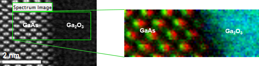
It is useful to perform atomic EELS analysis of oxides on II-V semiconductors to extract intensity line profiles from the As, O and Ga. In this example, you can clearly resolve the dumbbell structure of GaAs (left hand side of color map), plus the Ga and As atomic columns are visible. The interface region also shows the presence of Ga2O monolayer responsible for keeping Fermi level unpinned, which allows the electronic device to be turned on or off. Top left image: annular dark field (ADF) STEM survey image. Top right image: EELS color map. Ga: green, As: red, O: blue. Sample courtesy of University of Glasgow Microscope courtesy of Dr. Yan Xin at Florida State University, Tallahassee, FL. Acknowledgement to Dr. Toshiro Aoki at Jeol USA (now at ASU) for helping set up the microscope for the experiment.
Chemical analysis
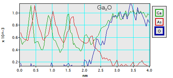
Insight into a molecule’s state, density and atomic distribution are valuable attributes to accurately characterize the chemical state of your semiconductor device. The spectrum image of an elemental map below shows how you can combine multiple techniques (energy loss near edge structure (ELNES), energy loss fine structure (EXELFS), and an atomic-specific radial distribution function (RDF)) to better understand the chemical state and shifts within a band structure.

Robustness and ease of analysis
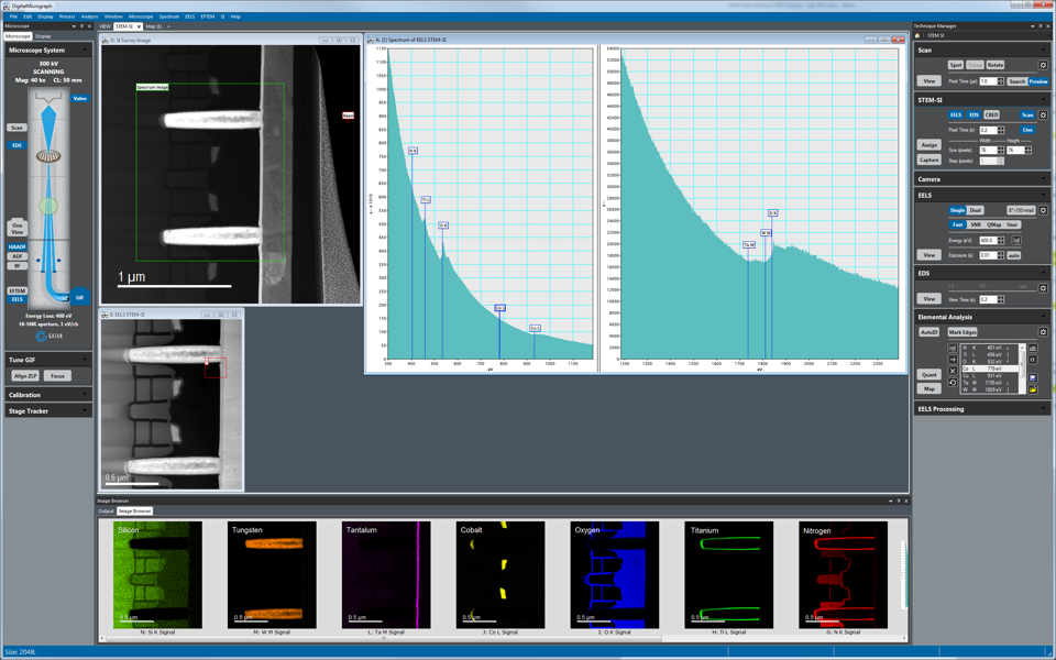
Gatan Microscopy Suite® (GMS) provides you with a reproducible way to analyze semiconductors with ease. GMS offers a complete re-visioning of electron microscopy's leading software with a simplified user interface and experimented oriented workflows. This software offers fully interactive user interface and microscope, streamlined data handling with technique based workflow, and user friendly EELS and EDS quantification to make sure your results are the focus, not the process to get them.