An example of why it is so important to correlate the structural and optical properties of semiconductor nanorods directly
Gatan instrument used
Gatan cathodoluminescence products enable optically-coupled transmission electron microscopy to reveal nanoscale structural, optical, and electronic properties.
Background
The size, shape, and structure of nanoparticles (NPs) are known to modify their functional properties, such as their electrical or optical characteristics. The development of commercial devices built by NPs depends critically on the ability of scientists and engineers to understand the relationship between structure and function. To this end, electron microscopy and optical emission spectroscopies, e.g., photoluminescence (PL), are commonly employed; electron microscopy is used to determine the size, shape, composition, chemistry, and presence of crystal defects of individual NPs at or near atomic resolution and PL used to determine band gap, electronic structure, and electric field. This approach has demonstrated its usefulness. However, the PL technique typically measures the average properties of many hundreds of NPs simultaneously, and there is a growing realization that the very different sample sizes used in the two techniques may lead to unsound conclusions.
Cathodoluminescence (CL) – luminescence initiated by electron excitation – is a particularly valuable characterization technique for NPs, bringing the power of optical emission spectroscopy to the electron microscope, enabling direct correlation of structure and function. CL also benefits from the ability to focus the electron beam to sub-nanometer dimensions, enabling the excitation of individual NPs and specific sites within an NP, such as a quantum dot, disk, or well-embedded within a semiconductor NP.
Nitride semiconductor nanorods (NRs) are highly attractive for applications, including high-efficiency light emission and hydrogen harvesting from the water. However, for commercial devices, manufacturing costs need to be reduced, but when doing so, this compromises the NR structural quality. The literature includes many reports of PL and electron microscopy studies of similar samples, though, critically, there is no direct correlation. Here, we demonstrate that direct correlation using cathodoluminescence measured in the transmission electron microscope (TEM) enables researchers to draw unambiguous and avoid incorrect conclusions.
Materials and Methods
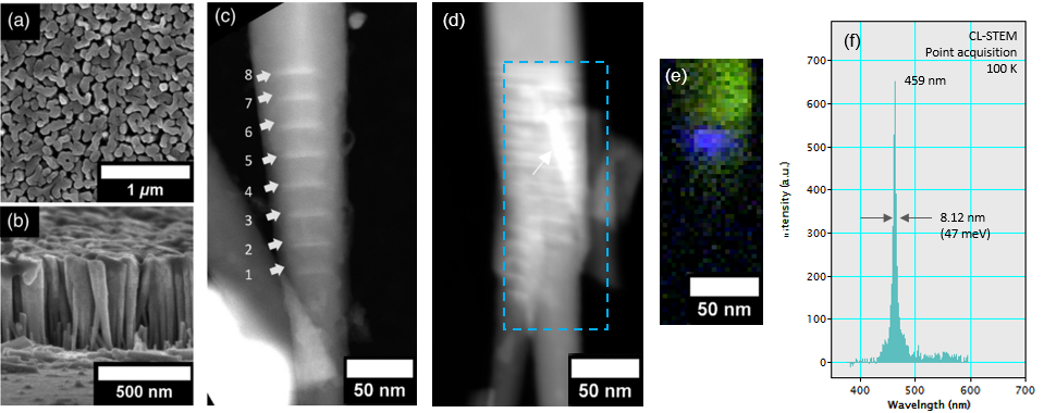
Previous studies revealed anomalous blue light emission from GaN NRs containing nominally 8, 3 nm thick In14Ga86N quantum disk (Qdisk) inserts grown by molecular beam epitaxy (500 – 600 °C). At these low growth temperatures, ~60% of the NRs exhibit ideal structures containing "perfect" InGaN Qdisks (Figure 1c). However, the remainder are of low quality with highly defective structures (Figure 1d). Analysis by PL revealed strong green and blue emission bands (550 and 460 nm, FWHMs 65 nm, respectively). The anomalous blue emission was concluded to be due to composition fluctuation within the InGaN Qdisks of the high-quality NRs; the low-quality NRs were thought to be too structurally poor to emit light efficiently.
The integral spectrum recorded by CL from hundreds of NRs replicated the spectrum observed by PL in previous work. However, an investigation by high spatial resolution CL demonstrated that only the blue emission band originated from low-quality NRs. Moreover, quantum dot (Qdot)-like emission centers emitting with a range of wavelengths (380 - 480 nm, FWHM 4 – 10 nm) were observed (Figure 1e) and could be correlated directly with small (<10 nm diameter) In14Ga86N nanoclusters formed unintentionally within the Qdisk region. This discovery could be an important step in producing solid-state quantum emitters for encryption and demonstrates the importance of correlating structural and functional properties in nano-objects.

Summary
Through the use of optically-coupled transmission electron microscopy, the mechanism of anomalous blue emission from nitride semiconductor NRs was revealed to be due to the unintentional fabrication of solid-state quantum dots in highly defective NRs. This contradicts previous studies, which had drawn erroneous conclusions and demonstrated the need to correlate structural and functional properties directly.
Credit(s)
A special thank you to A. Prabaswara and Prof. Boon Ooi, King Abdullah University of Science and Technology (KAUST) and the Experimental Technique Centre, Brunel University. For further information, see Prabaswara et al. J. of Nanophotonics, 11(2), 026015 (2017).
The Photonics Laboratory, KAUST aims to deliver compact and energy-saving integrated laser-diode-based devices and solutions for applications requiring light spanning the ultraviolet to the visible and near-infrared regime. A plethora of practical laser-based solutions are conceived, and proof-of-concept models are built for data collection and testing of a new class of innovative multi-function laser devices.