差分相位衬度
在原子尺度上针对电场和磁场的可视化和测量在材料科学发展中至关重要,因为它们直接影响材料的电子特性和具体应用(例如:存储技术或光电子学)。扫描透射电子显微镜(STEM)中的差分相位衬度(DPC)成像允许我们以极高的分辨率(受STEM仪器功能限制)来检查样品内部和外部的场。
援引 Dekkers 和 de Lang [N. H. Dekkers and H. de Lang, Optik 41, 452 (1974)]的工作,DPC依赖于探测器平面上电子斑照明强度的质心(COM)位移(也称为汇聚束电子衍射(CBED)图或朗奇图)。这种质心的横向偏移是由于电子探针动量变化引起的,并且与局部电场成负比例关系。
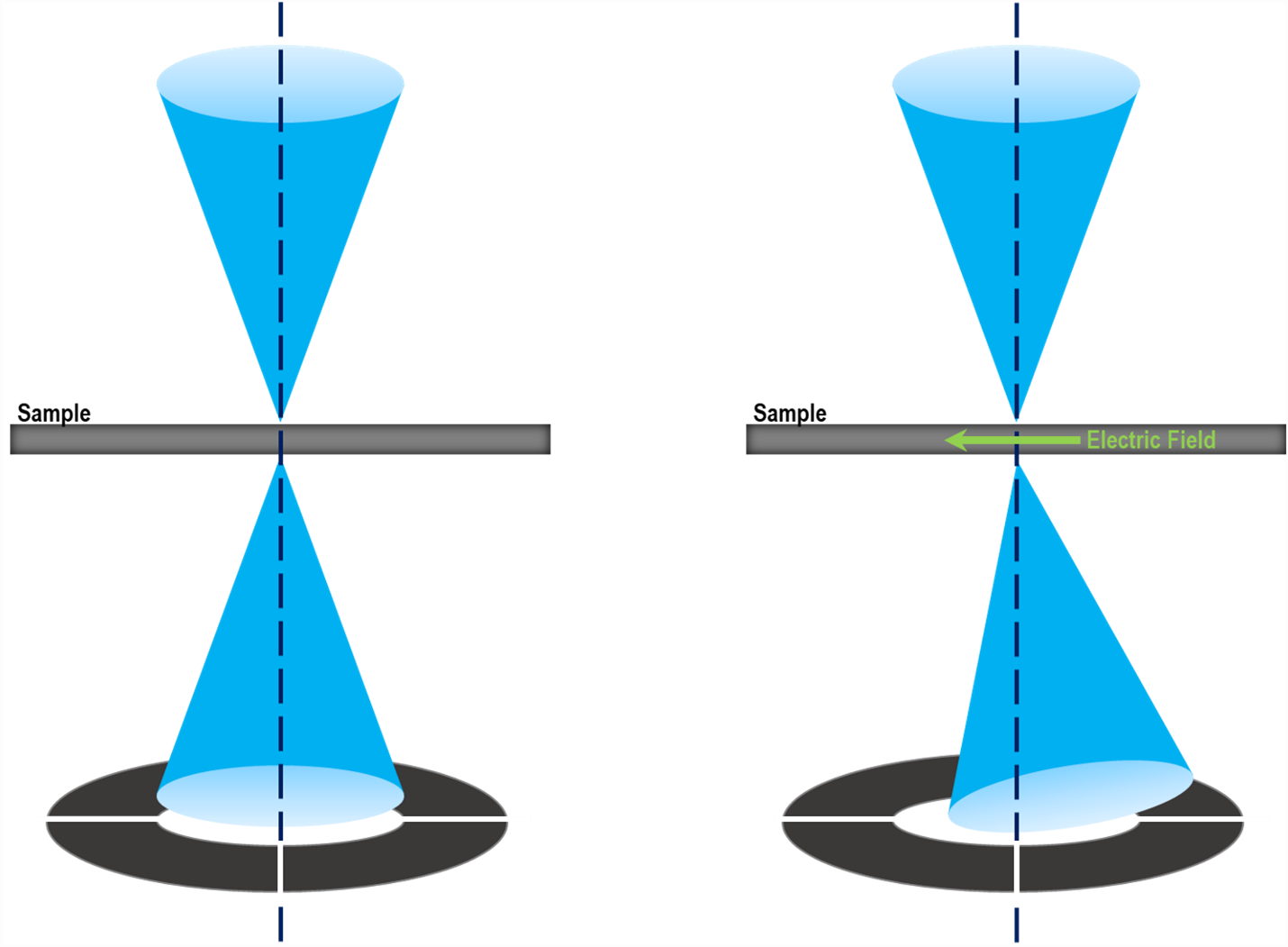
对于非磁性样品,假设电子束通过路径的电场变化很小,并且电子束在穿过样品厚度时展宽较小,则可以应用这种线性关系并使用测得的电子束偏移来计算局部电场:

ΔPxy: 电子束动量的变化,Exy:电场,Δz:样品厚度, Exy: 电场, Δz: 样品厚度, vz 电子沿电子束方向的速度。
一旦计算出电场,还可以通过计算电荷密度的散度来确定电荷密度(根据高斯定律,电场的散度与电荷密度成正比)。
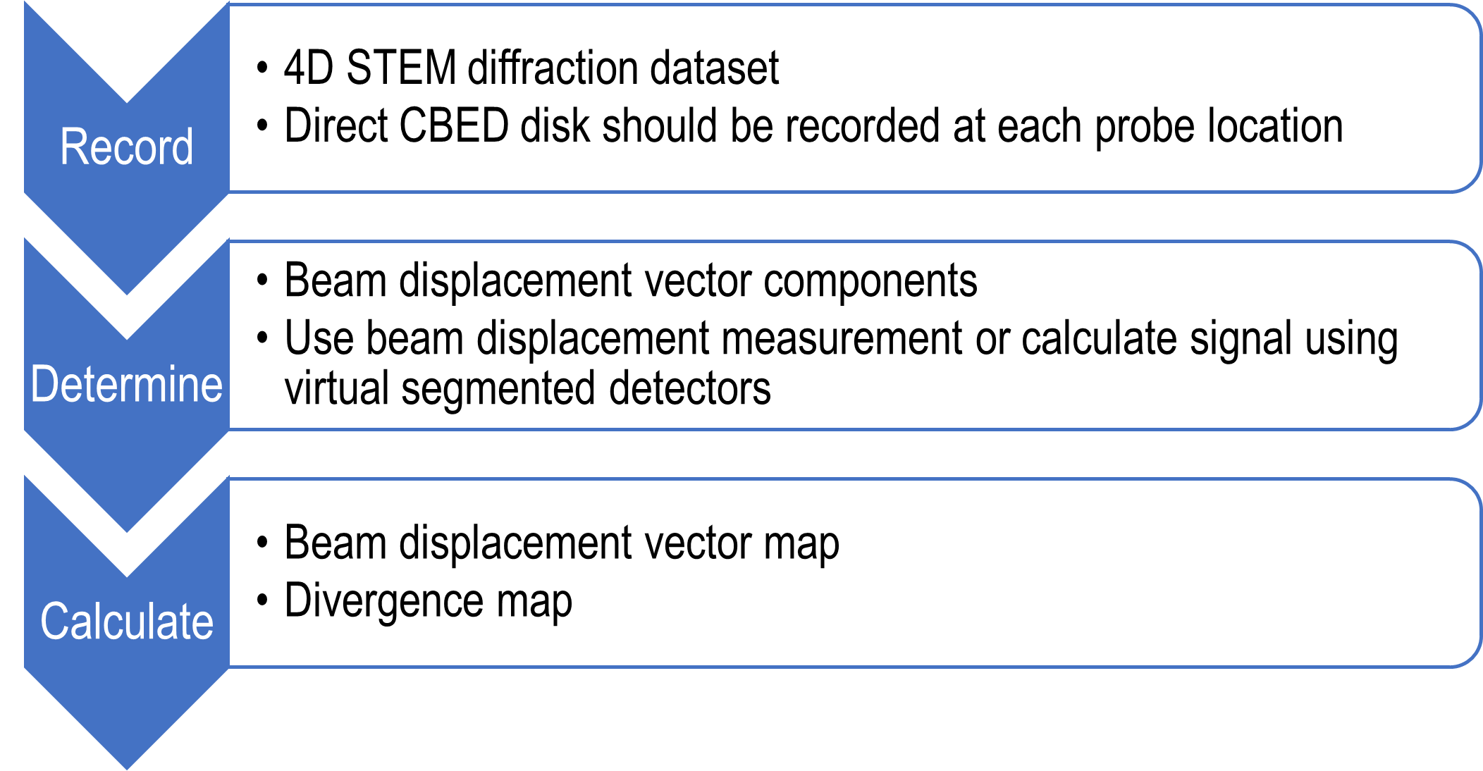
传统的DPC成像包括在电子显微镜中安装物理分割STEM探测器并测量落在相对分割片段上的强度差以测量电子束偏移(1977)。在这种配置中,选择合适的相机长度以确保在每个探头位置有足够的信号落在每个分割探头上至关重要,然而每个分割探头内的强度变化不会被捕获,因为每个分割探头都会在其整个区域上积分信号。另一个缺点是信息传输效率在多个空间频率上的限制 (Optik, 54, 83-96, 1979)。4D STEM DPC 通过记录每个探头位置的整个衍射图来克服这些限制。随着像差校正STEM和高速直接检测像素化相机的商业化,4D STEM DPC 成像成为薄样品原子分辨率电场测量的常用方法。它可以在DigitalMicrograph®中完成,如下方的流程图所示:
4D STEM DPC的数据收集注意事项
与任何电子显微镜技术一样,显微镜设置和样品对于DPC电场测量至关重要。在这种情况下,在每个STEM探针位置记录会聚束电子衍射(CBED)。然后,应用图像处理来测量每个4D STEM数据块衍射花样中的电子束中心偏移,以计算电场。
汇聚角: 在理想情况下,STEM 探针应明显小于电场变化的尺度。探头尺寸(空间分辨率)由会聚角(聚光镜光阑和镜筒配置)决定。较大的汇聚角会提供较小的STEM探针(更好的空间分辨率),反之亦然。对于原子分辨率DPC,当探针尺寸小于特征尺寸时,可以将样品电势视为线性。在这个近似值中,测量与样品电势强度成正比的相位,得到的衍射是均匀移动的原始衍射盘。如果探针尺寸大于要测量的特征,则DPC信号是由原始衍射盘中的偏移和强度重新分布引起的。该信号包括有关短程和长程电势的信息,可以通过应用频率滤波来解卷。/p>
相机长度: 选择允许您在CBED中录制完整中心电子束的相机长度。相机长度越长,衍射盘分布的像素数就越多,从而导致每个相机像素的信号较少。选择汇聚角时,还应考虑相机长度。
样品厚度: 测得的电场可能会受到厚度大于几纳米的样品的影响,因为在这种情况下,通过电子光路的电场略有变化和电子束通过样品厚度时的最小电子束展宽的假设不再有效。
在DigitalMicrograph 中计算DPC
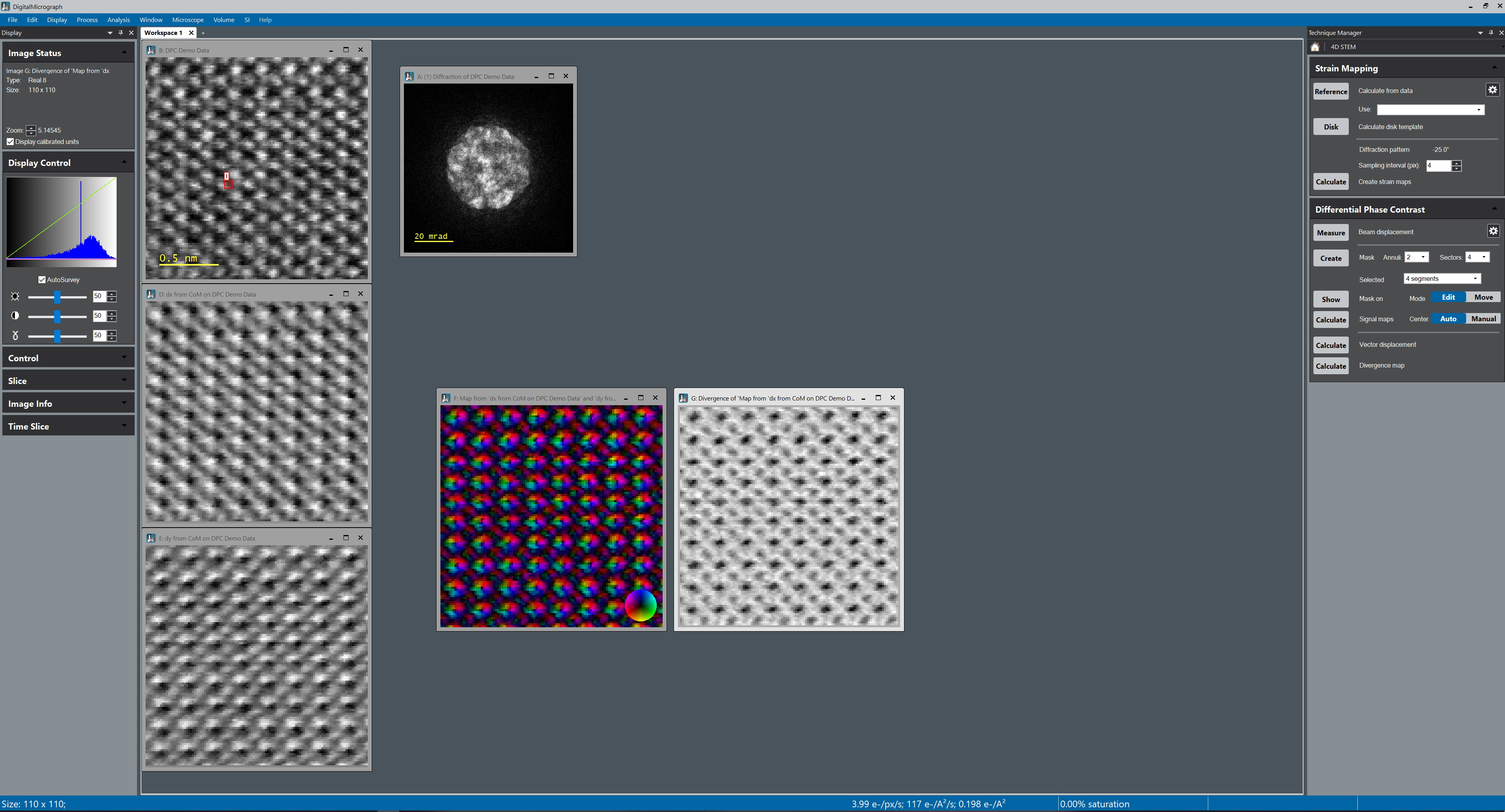
我们使用的样品数据由Molecular Foundry(美国加利福尼亚州伯克利)的研究人员提供,可在此处下载。 在300 kV下收集能量过滤的4D STEM衍射数据,GIF Continuum® K3® IS 系统使用电子计数模式,像素尺寸为0.2 Å,像素停留时间为0.00169 s。
DigitalMicrograph中的DPC计算是使用差分相位衬度技术和调色板在4D STEM衍射数据 (CBED)上完成的(下面的屏幕截图):
- 确定电子束位移矢量分量(采样平面上的两个正交方向x和y)。此处有两个选项可用:
- 质心(CoM)计算或互相关:
- CoM:DigitalMicrograph计算每个衍射花样(每个探针位置)的CoM,将其与参考衍射花样的CoM 位置(根据整个数据集计算)进行比较,并输出x和y方向上的偏移。
- 互相关:DigitalMicrograph将每个衍射花样(每个探头位置)与4D STEM数据中的中心花样互相关(使用可选的用户定义数值滤波器),并输出x和y方向上的偏移。
- 虚拟分割探测器:这类似于使用物理分割传统DPC的STEM探测器。用户无需在显微镜上安装探测器,而是在DigitalMicrograph中设计了一个虚拟探测器(包含多个环和段)。然后,软件会计算每个分割探头的每个衍射花样中的像素强度总和。然后,它输出用户定义的信号(应用于来自各个分割探头的信号的任何数学运算)。
- 质心(CoM)计算或互相关:
- 计算电子束位移矢量图和散度
选择两个正交分量,然后点击Calculate vector displacement。DigitalMicrograph输出矢量图,每个像素的强度和颜色分别对应于电子束位移矢量的大小和方向。最后,选择此矢量图,然后单击Calculate divergence map。根据上述方程,这些输出可用于计算电场和电荷密度。
致谢
Christopher Addiego,Wenpei Gao和Xiaoqing Pan(美国加州大学尔湾分校)为在DigitalMicrograph中开发和实施DPC技术提供了咨询。我们还要感谢Jim Ciston(Molecular Foundry, Berkeley, CA, USA)提供示例数据集,并感谢Roberto dos Reis(西北大学)提供建设性的反馈。