Ready, set, go! Ensuring an identical TEM specimen preparation route again and again
FePt films are very promising materials in the area of heat assisted magnetic recording (HAMR). These films require high bulk magnetocrystalline anisotropy energy constant and well isolated grains with a uniform size less than 6 nm. FePt thin films are prepared by RF sputtering on a Si substrate from a multi target, multi-layer sputtering system. The sputtering power, in-situ heating temperature and Argon gas pressure during this process are all parameters that may affect the microstructure (grain size), magnetic properties and ultimately applicability of these materials for HAMR. Thus, it is vital to study the effect of each of these processing parameters via preparation of multiple samples and modification of one parameter at a time. Since statistical data is required, transmission electron microscopy (TEM) and a technique that produces a large electron transparent area is needed. In this application note, we focus only on the specimen preparation technique for observation by TEM.
In order to make conclusive conclusions in comparison between these thin film samples, the preparation technique for TEM must minimize preparation induced differences. For observation in a TEM, specimens are prepared by various mechanical polishing steps and then Ar ion milling. It is well known that both mechanical and ion thinning can induce artifacts in the specimen. Thus, for the microstructure of different samples with varied process parameters to be compared by TEM, preparation to electron transparency needs to be identical for all of the specimens.
To achieve this goal, 3 mm plan view specimens were cut out from each material type, using a diamond scribe. These specimens were mechanically polished flat from the back side (Si substrate) to less than 100 µm and then further thinned to less than 15 µm in the dimpled area with a Gatan dimple grinder (again from the Si side). The specimens were then mounted on a clamp type DuoPost® (dimple side up) and inserted in the Precision Ion Polishing System (PIPS™) II. The X, Y stage in PIPS II makes it possible to center the dimpled area with respect to the center of rotation and center of the Ar ion beams to a few micrometers accuracy.
From TEM study of specimens made previously using an older model PIPS, we learned that polishing until perforation causes the areas around the hole to curl and makes it very difficult, or in some cases impossible, to image the region of interest in the TEM. In order to prevent this from happening, it is essential to control and stop the Ar milling just before perforation occurs. Use of the PIPS II enables constant monitoring of the remaining thickness and consistent halting of the milling process at the right point. Optical images were captured with the digital camera of the PIPS II, which captures and stores high resolution images from every rotation of the specimen during the milling process. In developing the preparation method, test specimens were mounted in the PIPS II and milled until perforation. After milling was complete, these sets of images were opened in a 3D stack to study the change in the appearance of the milled area in PIPS II with time/thickness.
As shown in Figure 1a, as the milling proceeds, the specimen thins and white light fringes appear in the center of the milled area and continue to grow outwards. We observed two deep purple fringes and then a yellow fringe before the center area turned gray/black. After studying multiple specimens, it was concluded that perforation happens immediately after these fringes stop appearing in the center and this area starts to turn dark gray/black (Figure 1c). Ion milling was done from the back side of these specimens: we believe most of the Si substrate is removed by milling and only the FePt thin film remains.
 Early stages of milling, white light fringes start to appear. (b) Mid stages of milling, white light fringes grow from inside the milling area toward the outside. (c) Right before perforation: fringes stop growing and milling area starts turning dark gray/black.")
Based on these observations, both guns were set to mill at 9° Top and 3.5 kV energy. Milling was performed with double beam modulation to prevent DuoPost clamp material being sputtered on the specimen. Milling was started and continued until white light fringes were observed in the PIPS II camera image (Live Mode). Milling angle and beam energy were then reduced to 7° Top and 2.5 kV, respectively, until the first deep purple fringe was observed as seen in Figure 1a. Milling angle and beam energy were then reduced to 6° Top and 1.0 kV until the second deep purple fringe appeared. Milling was continued at 6° Top and 0.1 – 0.5 kV until most of the Si substrate was removed and the milling area started to turn color to dark gray/black. Figure 2, shows PIPS II camera images of two other specimens right after milling was stopped.

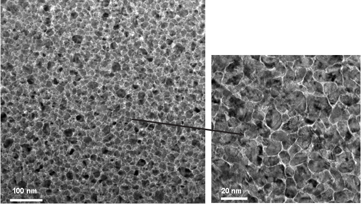
Specimens were then removed from PIPS II and imaged in TEM (Figure 3). After observation of specimens from various samples, prepared as described, the effect of power, temperature and pressure was characterized on the microstructure of FePt films [Granz and Kryder 2012; Granz, Barmak and Kryder 2012].

In conclusion, several features in the PIPS II were used to make identical preparation route of multiple specimens:
- X, Y stage movement made it possible to bring the dimple area of each specimen to the center of rotation with a few microns accuracy
- The automated gas flow control made it possible to run the ion guns at optimized conditions and consistently repeat the same conditions from specimen to specimen
- Low energy milling (0.1 – 0.5 kV) made it possible to mill most of the Si substrate without perforation and still have an electron transparent region with reproducible results
- Observation of 3D image stacks of previously made specimens, made it possible to learn about the milling characteristics of the material (change in white light fringes and perforation)
- Observation of the specimen in PIPS II camera Live Mode, with knowledge of its milling characteristics, made it possible to stop milling at a specific point (right before perforation)
References
- S. Granz and M. H. Kryder, Journal of Magnetism and Magnetic Materials 324 (2012) 287.
- S. Granz, K. Barmak and M. H. Kryder, Journal of Applied Physics 111 (2012) 07B709.