What is EDS?
One of the many types of signals generated in a scanning transmission electron microscope (STEM) is characteristic x-rays: incident electron creates a vacancy in an inner orbital of the atom, then an electron from a higher orbital fills this vacancy and emits x-rays. '
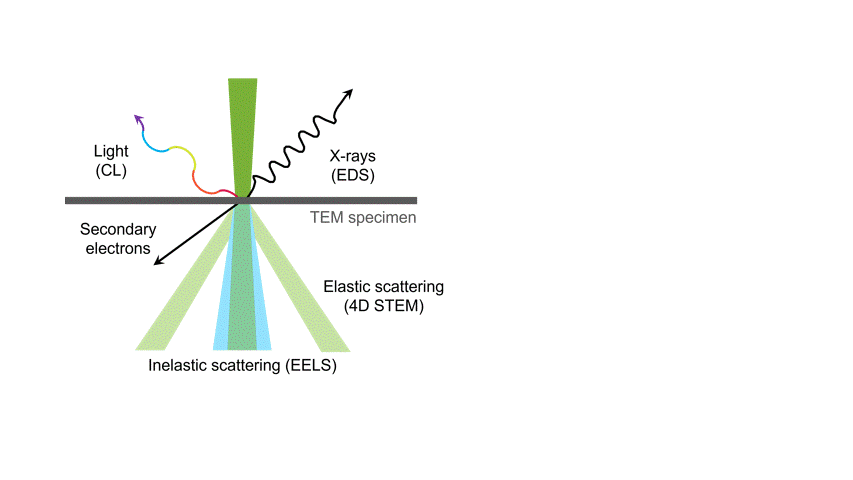
Energy dispersive x-ray spectroscopy (EDS, EDX, XEDS, etc.) is an analytical technique that uses these characteristic x-rays for elemental and compositional analysis of materials. Unlike electron energy loss spectroscopy (EELS), EDS requires minimal setup on the microscope, is used on semi-thin to bulk specimens, and offers a high signal-to-background ratio. This technique is key to understanding foreign materials, coating compositions, small component materials, evaluating corrosion, phase identification, and distribution.
Gatan offers eaSI™ EDS, the most effective and efficient STEM EDS that leverages the EDAX Elite T EDS detector and DigitalMicrograph® software.
Since the changing local chemical environment atomic bonding has little effect on EDS, there are better techniques than this one for specimen chemical analysis. However, it is excellent to determine the elemental distribution of a sample. Combined with electron energy loss spectroscopy (EELS), you can easily analyze your specimen's chemical and compositional makeup.
Unlike similar techniques, EDS requires minimal setup and is used in semi-thin to bulk specimens; thickness options are unlimited. EDS also offers a high signal-to-background ratio (SBR). Some limitations of EDS include non-local fluorescence; low-Z limits; and limited thin-film signal-to-noise ratio (SNR).
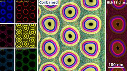
In the example below, the Sr L2,3-edges at 1940 eV were not within the 0 – 850 eV energy range (top) after an EELS analysis was run on a semiconductor sample. When spectrum imaging was used to obtain the EDS Sr elemental map in combination with the EELS Ti, Fe, and La maps (bottom), the collective color map shows the distribution of each element across an extended energy range.


For more information about comparing this technique to other analytical techniques, please visit EELS.info, an educational site.


Gatan Microscopy Suiteとしても知られるDigitalMicrographソフトウェア。デジタルカメラの制御と共に、電子線トモグラフィ、その場観察、スペクトラムイメージング、ディフラクションイメージング、その他多くのアプリケーションをサポート。


EDSシステム")
EDAX Octane Elite SDDの革新的な進歩が検出器テクノロジーを次のレベルに進めます。この検出器のシリーズは、軽元素検出のための低エネルギー感度と低電圧マイクロアナリシスを目覚しく向上させる、新しいシリコンナイトライド (Si3N4) 製ウィンドウを採用しています。

最新のシリコン ドリフト検出器 (SDD) 技術と高速エレクトロニクスを組み込んだ、強化されたエネルギー分散型 X 線分光法 (EDS) プラットフォームです。

コンパクトなパッケージで強力なエネルギー分散分光法 (EDS) 分析機能を提供し、合理化された操作で迅速な結果と使いやすさを保証すると同時に、パフォーマンスと柔軟性を最大限に高めます。

 システム")
エネルギー分散型 X 線分光法 (EDS)、電子後方散乱回折法 (EBSD)、波長分散型分光法 (WDS) の最新技術を 1 つの分析ツールに統合します。
 システム")
 システム")
EDAX Neptune は、エネルギー分散分光法 (EDS) と波長分散分光法 (WDS) の分析技術を単一のプラットフォームに統合することにより、EDS のパワーと柔軟性に加え、WDS の解像度、精度、検出限界も提供します。