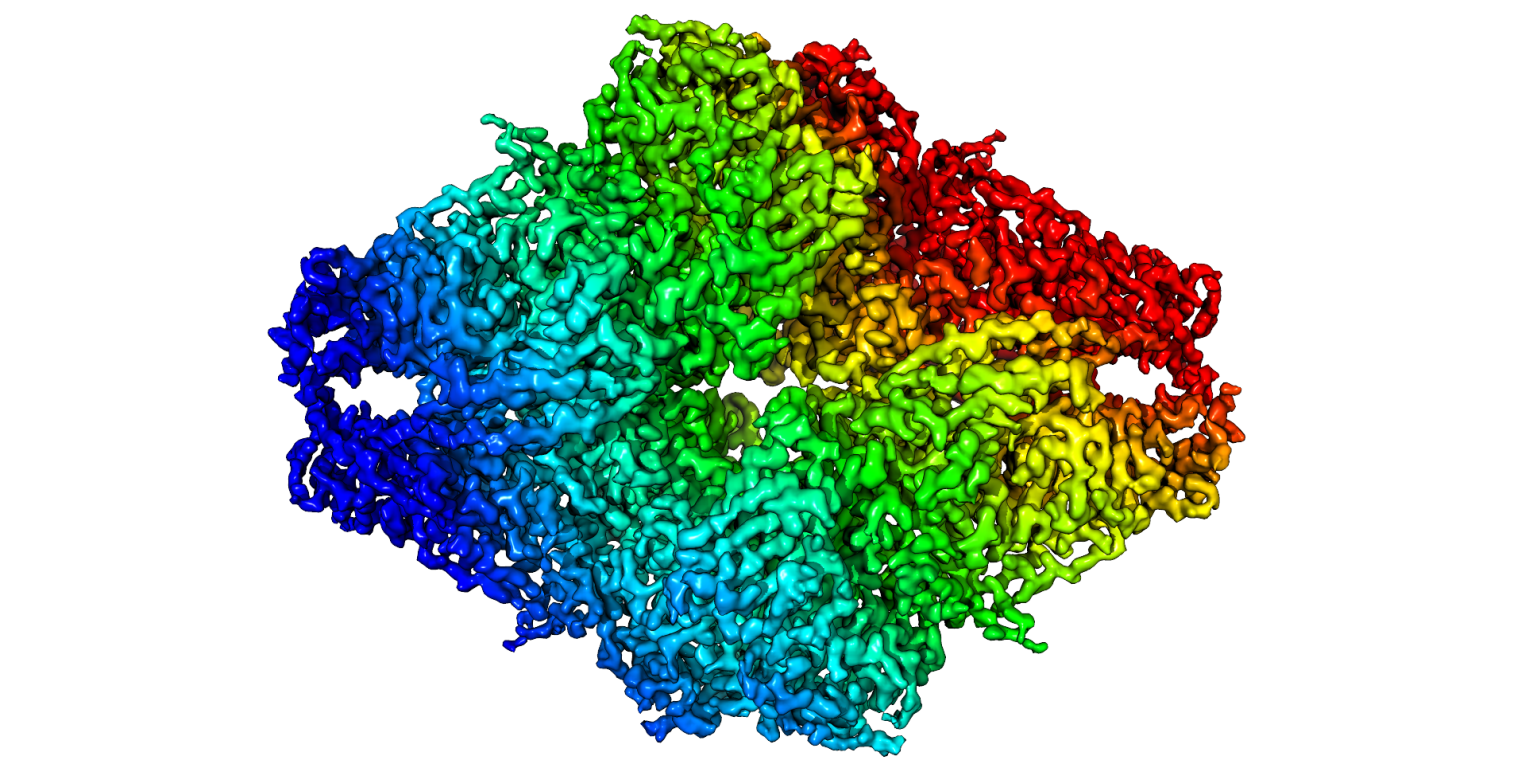
First 3.2 Å β-galactosidase structure solved by cryo-EM
Bartesaghi, A.; Matthies, D.; Banerjee, S.; Merk, A.; Subramaniam, S.
Structure of Escherichia coli β-galactosidase (∼465 kDa) at 3.2 Å resolution solved using the GIF Quantum LS energy filter that includes a K2 Summit camera. The first atomic model derived using single-particle cryo-EM analysis closely matches the 1.7 Å crystal structure with a global rmsd of ∼0.66 Å. Proc Natl Acad Sci U S A. 2014 Aug 12;111(32):11709-14.
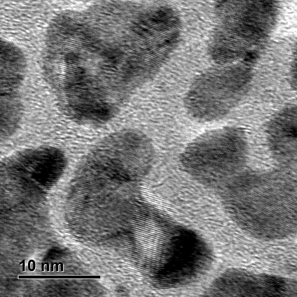
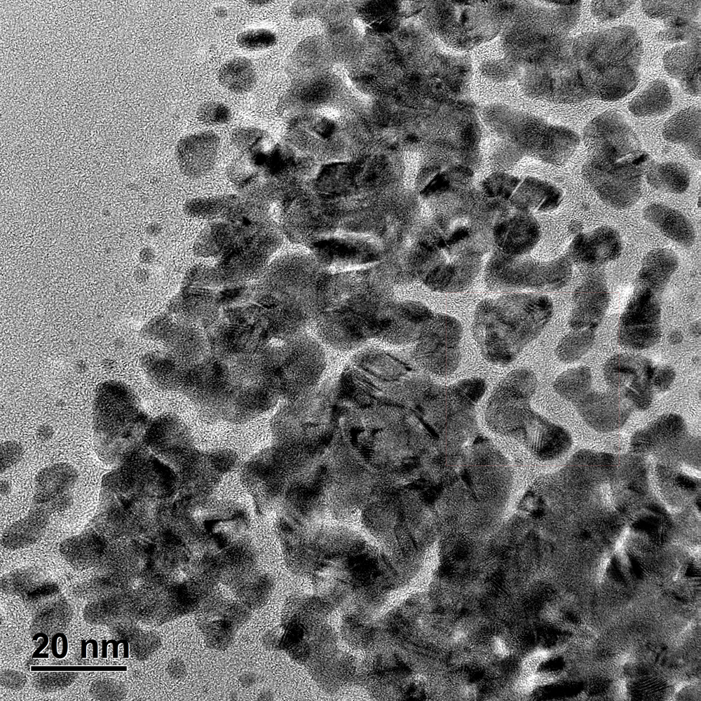
High resolution image of Au nanoparticles, drift correction off (image 1)
Image of gold (Au) nanoparticles shows the impact sample motion may have on an image when drift correction is turned off. See High-resolution image of Au nanoparticles, drift correction on (image 2 and 3) in the OneView media library to see how OneView minimizes the impact of sample motion when drift correction is turned on.
TEM magnification: 255kx; electron energy: 200 keV; exposure time: 2.56 s; drift correction: off
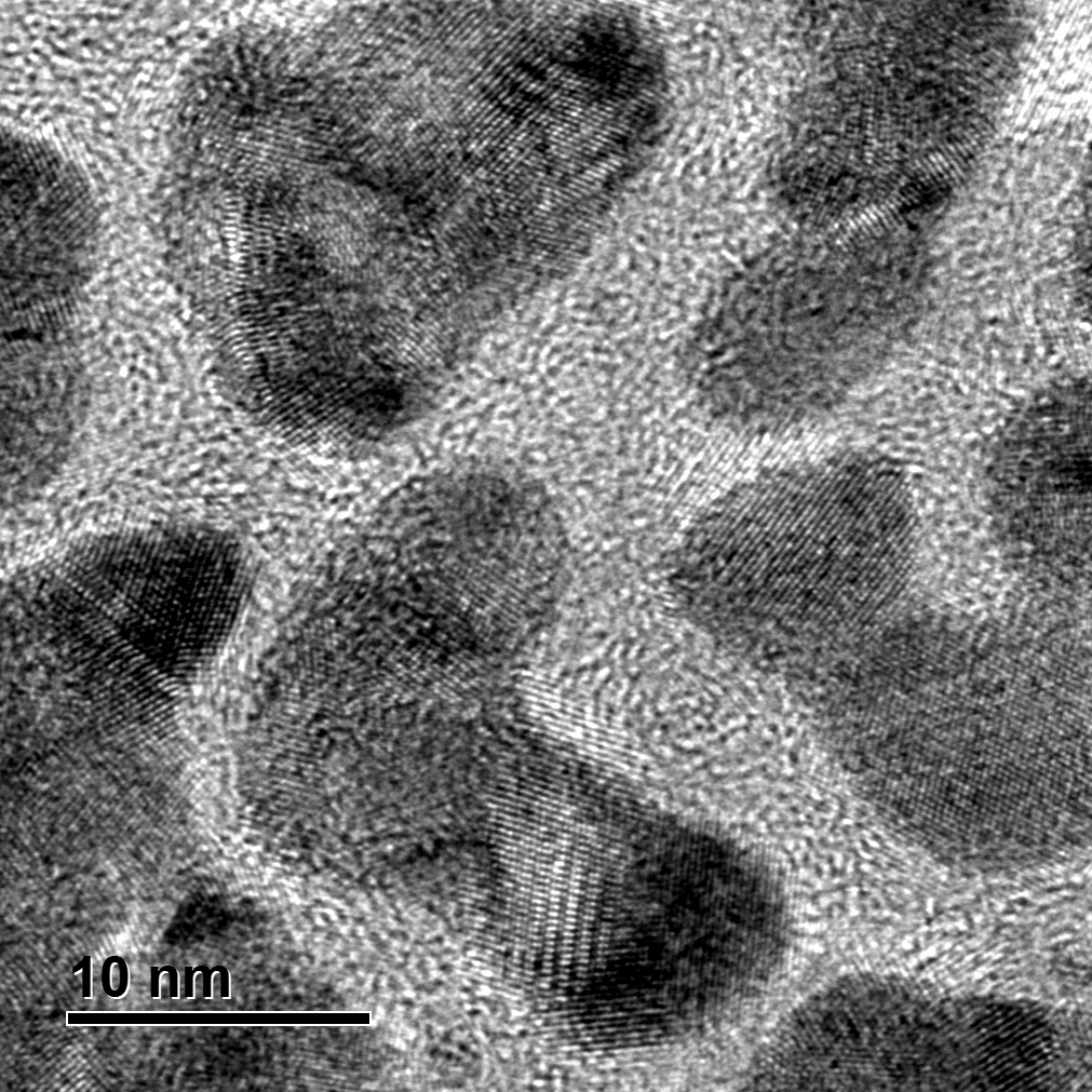
High resolution image of Au nanoparticles, drift correction on (image 2)
Image of gold (Au) nanoparticles shows how OneView minimizes the impact of sample motion when drift correction is turned on. See High-resolution image of Au nanoparticles, drift correction on (image 1) in the OneView media library to see motion of the original sample when drift correction is turned off.
TEM magnification: 255kx; electron energy: 200 keV; exposure time: 2.56 s; drift correction: on
High resolution image of Au nanoparticles, drift correction on (image 3)
Image of gold (Au) nanoparticles shows how OneView minimizes the impact of sample motion when drift correction is turned on. See High-resolution image of Au nanoparticles, drift correction on (image 1) in the OneView media library to see motion of the original sample when drift correction is turned off.
TEM magnification: 255kx; electron energy: 200 keV; exposure time: 2.56 s; drift correction: on
[110] CBED pattern of GaN/InGaN
OneView camera is able to synchronize frames for 4D STEM applications. Image is related to [110] high resolution image of GaN/InGaN image in the OneView media library.
Camera length: 550 mm; electron energy: 200 keV; exposure time: 5 s; pattern is displayed on linear scale
[110] CBED pattern of GaN/InGaN
OneView camera is able to synchronize frames for 4D STEM applications. Image is related to [110] high resolution image of GaN/InGaN image in the OneView media library.
Camera length: 550 mm; electron energy: 200 keV; exposure time: 5 s; pattern is displayed on logarithm scale
Y2Ti2O7 results on PECS II system
A. Secondary electron B. IQ EBSD map C. IPFZ map
TRIP steel results prepared on PECS II system
Results courtesy of Dr. Francois Brisset and Yoann Angilella of Electron Microscopy Department, ICMMO, CNRS- University of Paris- Sud. Data acquired with a Zeiss Supra & Sigma HD and EBSD with Hikari XP and OIM from TSL-EDAX.
A. Secondary electron; (B) EBSD image quality map; (C) IPFZ map
Zircaloy 2
Results courtesy of Department of Materials, University of Oxford. Professor Angus Wilkinson and Dr. Hamidreza Abdolvand. Data acquired on a Zeiss Compact Merlin equipped with a Bruker Quantax EBSD System.
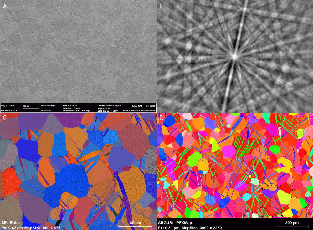
(A) Secondary electron image of the surface of highly stressed Zircaloy 2 alloy showing twin boundaries; (B) BSED Kikuchi pattern of sample; (C) EBSD Euler angle map; (D) IPFZ map, FOV 1 mm x 0.7 mm
High resolution observations of interface dynamics using a direct electron detection camera
Data courtesy of National Center for Electron Microscopy, LBNL, Berkeley, CA, USA and Faculty of Technology & Metallurgy at U. of Belgrade, Serbia.
4/6 Multilayer step—Last 0.05 s
- Step height n/m=4/6 – 4 planes in lower grain meet 6 planes in the upper grain
- Preserved ABAB…stacking sequence over the step interface
- Buried step parallel to the surface forms during step migration (b-d)
- “Shadow” of the step most likely due to remanence at the surface (e)
This work is supported by DOE/BES/MSD under Contract No.DE-AC02—05CH11231.
Pages

![[110] CBED pattern of GaN/InGaN [110] CBED pattern of GaN/InGaN](https://www.gatan.com/sites/default/files/CBED-3-5-sec-spot-8-cl-550mm-081914-%28good%29-central-2k.png)
![[110] CBED pattern of GaN/InGaN [110] CBED pattern of GaN/InGaN](https://www.gatan.com/sites/default/files/CBED-3-5-sec-spot-8-cl-550mm-081914-%28good%29-log-scale.png)


