Application of PIPS II system for cross-sectional TEM specimen preparation of semiconductor devices
Helmholtz-Zentrum Berlin für Materialien und Energie
Institute Nanoarchitectures for Energy Conversion
Hahn-Meitner-Platz 1
D-14109 Berlin Germany
At Helmholtz-Zentrum Berlin für Materialien und Energie GmbH (HZB, formerly known as Hahn-Meitner Institute, HMI), Berlin, Germany, a specific technique for the cross-sectional specimen preparation for transmission electron microscopy (TEM) has been developed during the recent years, mainly applied to thin film stacks of solar-cell devices. This approach consists of mechanical and argon (Ar) ion polishing of cross-section specimens, formed by face-to-face gluing of two thin film stacks using epoxy glue.
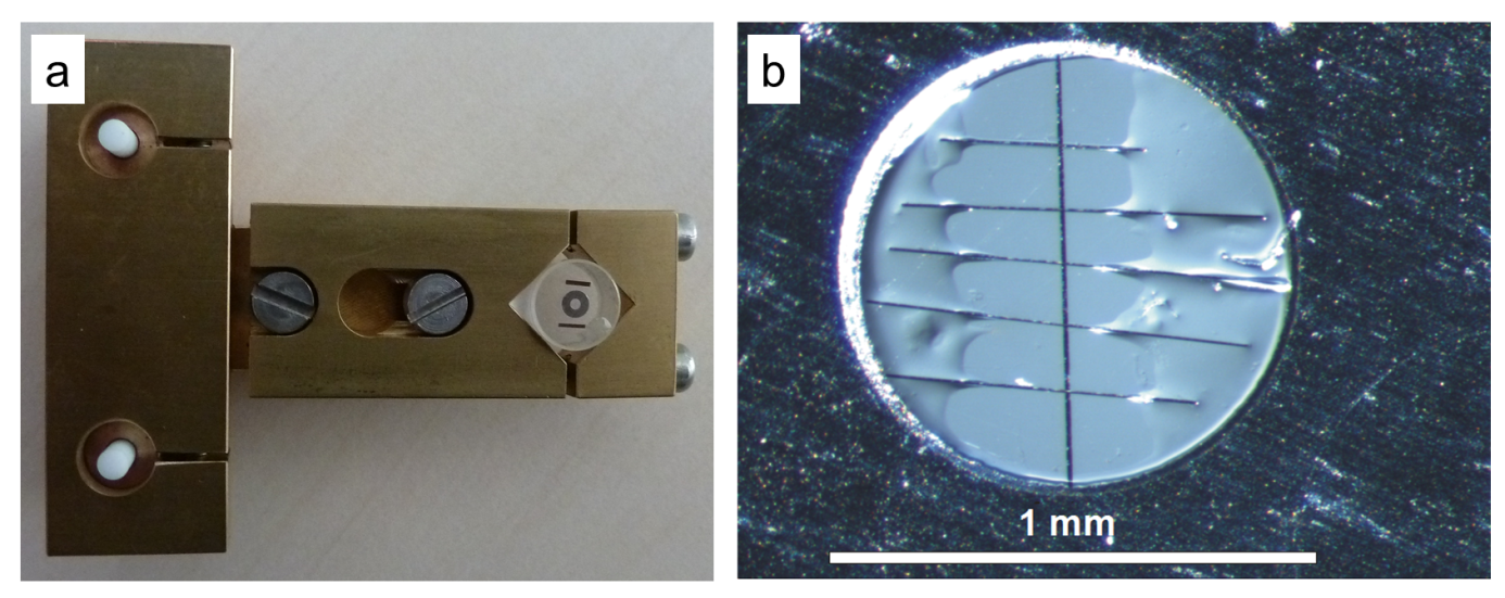
An important utility for the mechanical polishing of cross-section specimens is the T-Tool introduced by H. Zang in 19981, which is similar to the more familiar Tripod2. The T-Tool has been developed further by Peter Schubert-Bischoff at HMI/HZB, nowadays adapted and applied by numerous labs all over the world. Figure 1a shows a photograph of the T-Tool (HMI style) with a glass cylinder attached to it.
The mechanical polishing procedure involves lapping the cross-section specimen on diamond foils at various sizes of the diamond particles, gluing of a stabilizing metal ring on top of the polished specimen, as well as placing carbon fibers across the interface region of the cross-section (see Figure 1b).

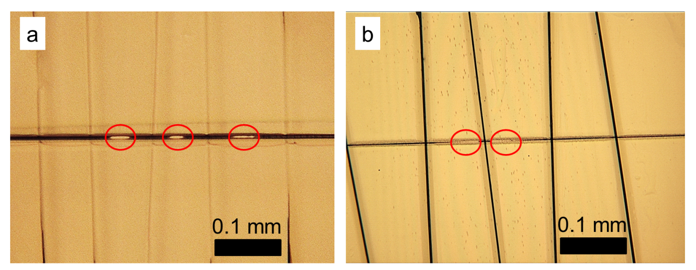
These carbon fibers exhibit a specific role during the Ar ion milling step of the preparation procedure, acting as screens for the ion beams. Consequently, regions in between the carbon fibers are milled more preferentially, which leads to not only one but several positions at which the specimen becomes transparent to the electron beam (see positions highlighted by red ellipses in Figure 2a). Also, the specimen may be Ar ion polished several times, maximizing the number of positions for each specimen at which TEM analyses may be conducted.
However, it is often a prerequisite for a TEM study to analyze a specific position in a material. The X,Y stage of the PIPS II system permits alignment of the Ar beams to region of interest on the sample. As a result, individual regions in between the carbon fibers can be milled (see Figure 2b).

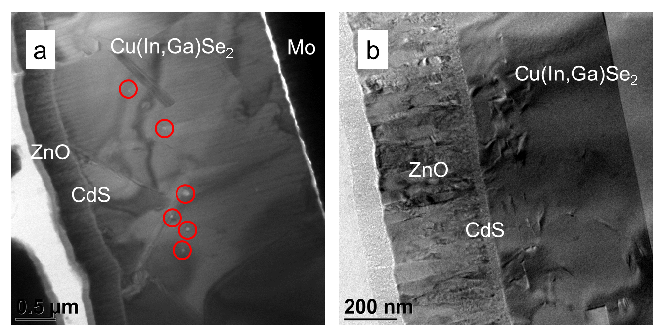
The improved specimen preparation approach described above was used to prepare cross-section specimens of a ZnO/CdS/Cu(In,Ga)Se2 /Mo glass thin film solar cell. This material system requires a high standard of specimen preparation, with respect to the mechanically instable interface between Mo and Cu(In,Ga)Se2, and also since ion milling of Cu(In,Ga)Se2 is incongruent, leading to the formation of Cu agglomerates (highlighted by red circles in Figure 3a) on the specimen surface3. These agglomerates may be reduced considerably by the application of liquid N2 during the Ar ion milling in the PIPS II system (Figure 3b). A temperature of -40 °C was adjusted.

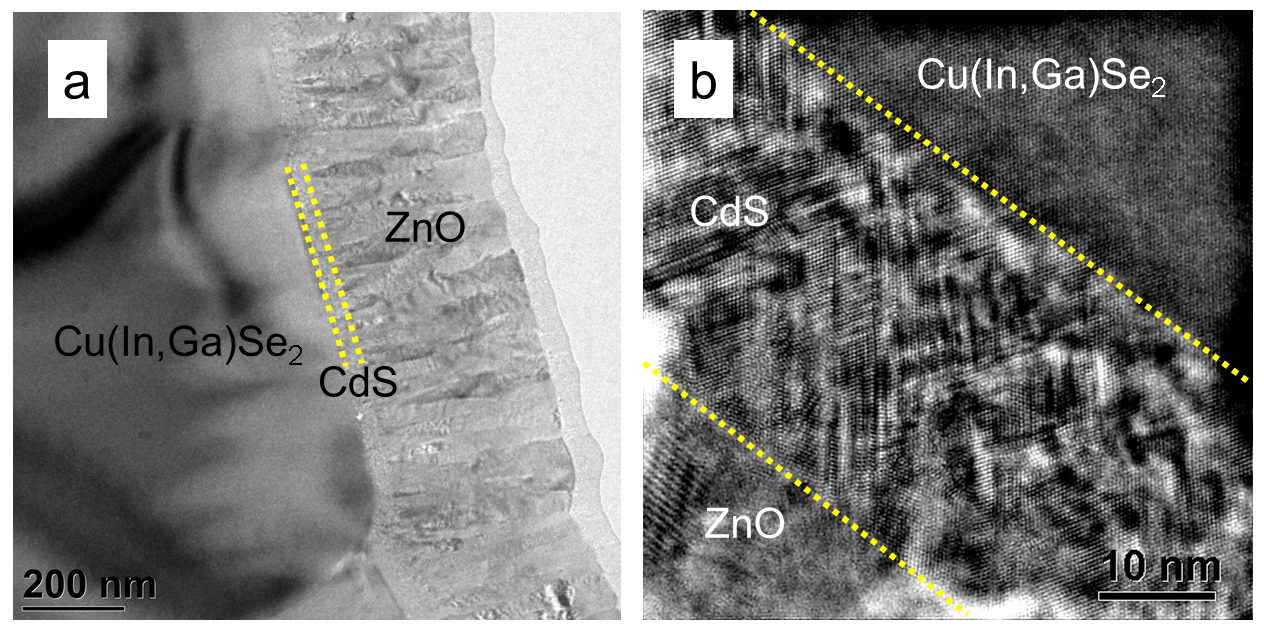
Within the ZnO/CdS/Cu(In,Ga)Se2 /Mo solar-cell stack prepared by use of optimized parameter settings, structural properties of the individual layers and their interfaces can be analyzed at high resolution (Figure 4).

Acknowledgements:
We would like to thank Dr. T. Rissom, HZB, for providing the solar cell.