Advantages:
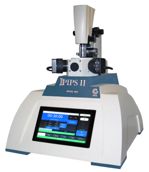
This revolutionary enhancement of the PIPS ion mill that has defined the standard for transmission electron microscope (TEM) sample preparation for over 20 years.
- X,Y stage permits alignment of argon beams to region of interest on the sample
- Improved collimated beam provides useable voltages as low as 100 volts for rapid and damage free preparation of FIB lamella
- Digital optical imaging with image storage and analysis in DigitalMicrograph® software
- 10" color touch screen for display and control of all PIPS™ II parameters


")


Science Direct
2022
Virtual and Physical Prototyping
2022
Model 695
Datasheet
Precision Ion Polishing System (PIPS) II
Applications
Protocols
Cleaning guns and cold cathode gauge
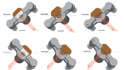
Stage and beam alignment
Lamella alignment
Lamella recipe
Related products
Dimple Grinder
Disc Punch
DigitalMicrograph® software
Disc Grinder
Ultrasonic Cutter