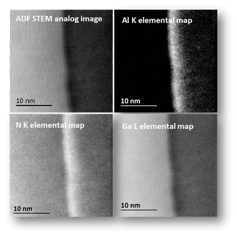
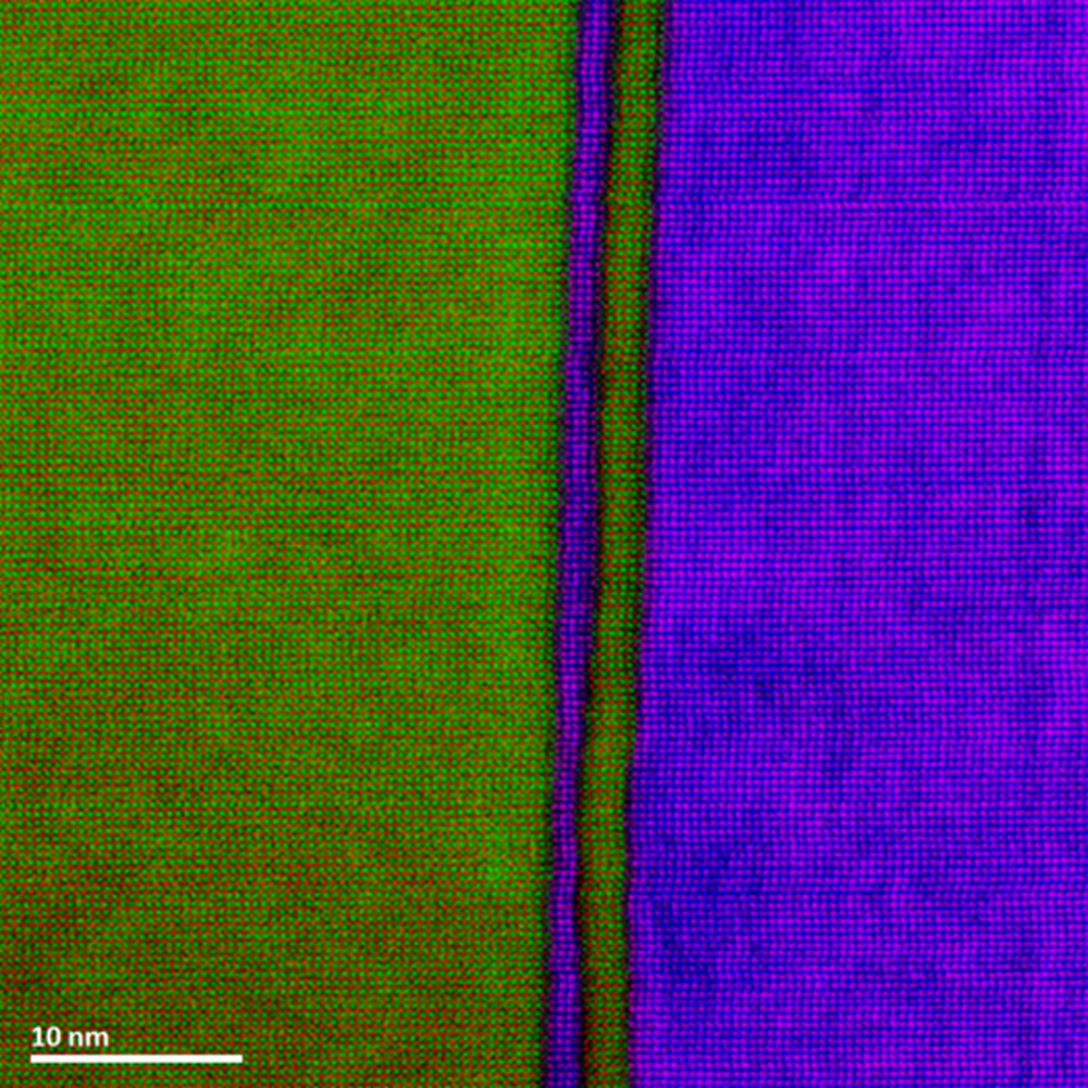
Fast atomic EELS analysis across the GaN/AlGaN interface
Paolo Longo, Ph.D., Gatan, Inc.
Sample courtesy of Dr. Giuseppe Nicotra at IMM-CNR, Catania, Italy
Microscope courtesy of Dr. Giuseppe Nicotra at IMM-CNR, Catania, Italy
Methods
probe-corrected ARM 200F TEM/STEM microscope
C-FEG emission gun
GIF Quantum® ER system
voltage: 200 kV
data taken in STEM mode
EELS core-loss spectrum (200 – 2200 eV) exposure time: 10 ms
beam current: 45 pA
dataset size: 250 x 250 pixels
total exposure time: 11 min
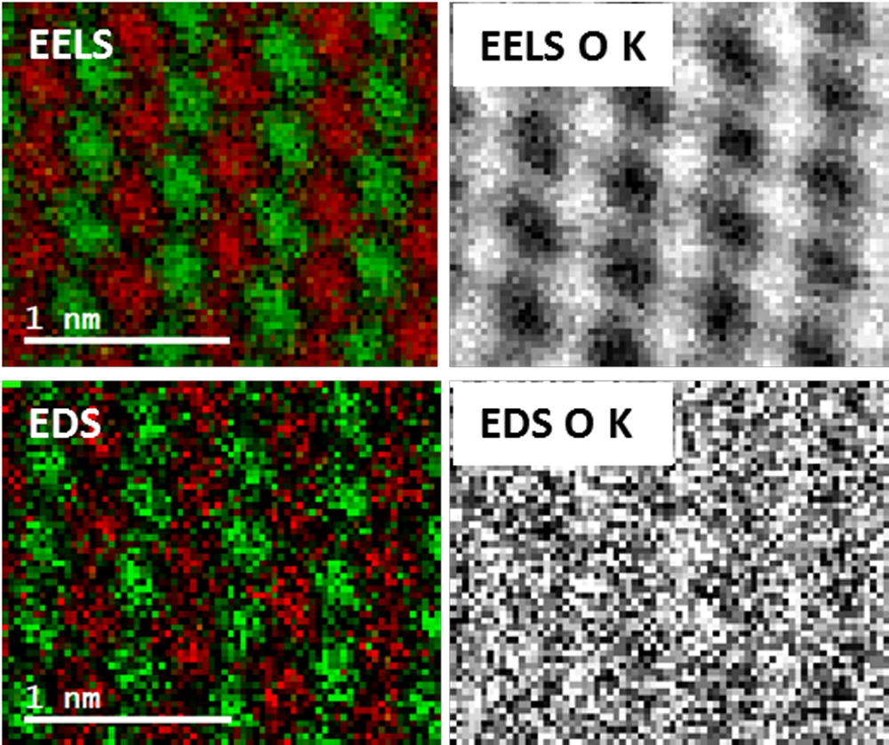
Fast Joint EELS / EDS color map of a SrTiO3 crystal
Paolo Longo, Ph.D., Gatan, Inc.
Sample courtesy of Dr. Yan Xin at Florida State University, Tallahassee, FL
Microscope courtesy of Professor Gerald Kothleitner, TU-Graz, Austria
Acknowledgement to Dr. Arno Meingast at CCEM, TU-Graz, Austria for helping set up microscope for experiment.
Methods
probe-corrected FEI Titan TEM/STEM microscope
X-FEG emission gun
GIF Quantum® ERS system
four quadrant SDD EDS detectors (FEI Chemistem)
Ti (green); Sr (red)
voltage: 200 kV
data taken in STEM mode
EELS low core-loss spectrum (300 – 2300 eV): 10 ms
dataset size: 70 x 57 pixels
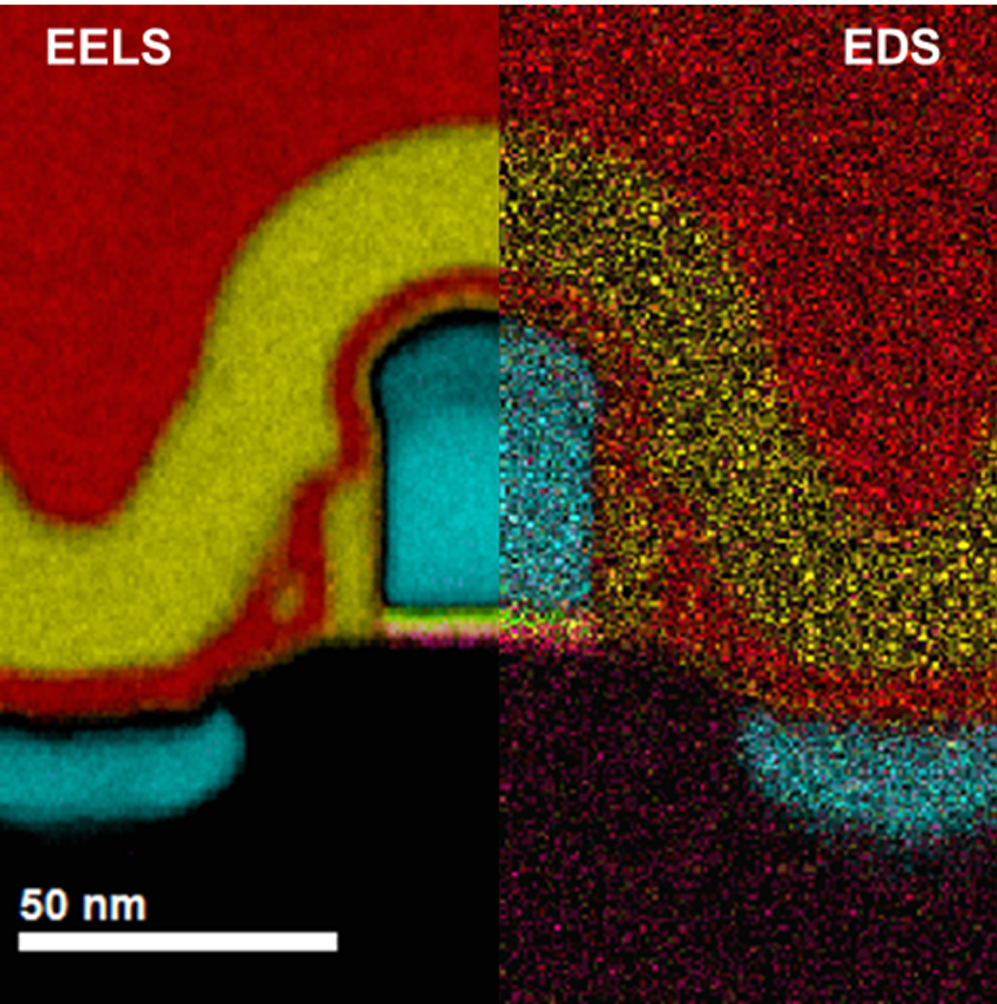
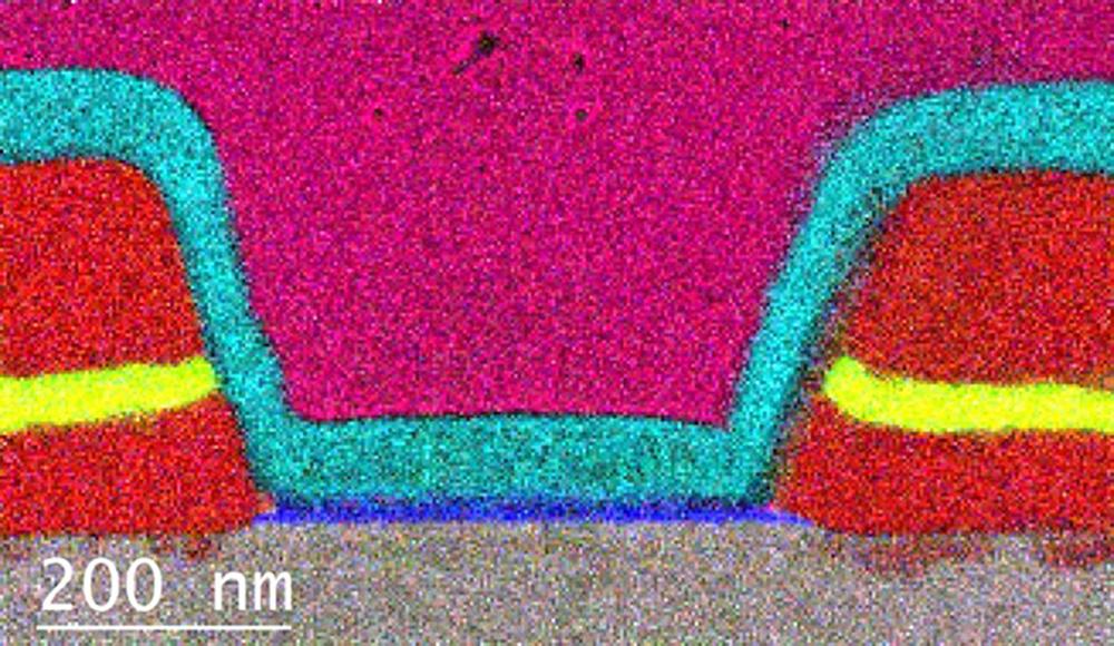
32 nm Transistor device
Paolo Longo, Ph.D., Gatan, Inc.
Sample courtesy of Dr. Pavel Potapov at Global Foundries, Dresden, Germany
Microscope courtesy of Dr. P. Rice and Dr. T. Topuria at IBM (Almaden), San Jose, CA
Acknowledgements to Dr. P. Rice and Dr. T. Topuria at IBM (Almaden), San Jose, CA for helping set up microscope for experiment.
Methods
probe-corrected Jeol ARM 200 TEM/STEM microscope
C-FEG emission gun
GIF Quantum® ER system
Jeol Centurio SDD EDS detector (0.98 sr)
O K at 532 eV (red); Ti L at 456 eV (green); Ni L at 855 eV (light blue); N K at 401 eV (yellow); Hf M at 1662 eV (purple)
voltage: 200 kV
data taken in STEM mode
EELS core-loss spectrum (300 – 2300 eV): 1.5 ms
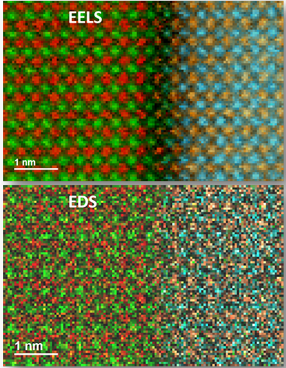
SrTiO3/LaFeO3 interfaces
Paolo Longo, Ph.D., Gatan, Inc.
Sample courtesy of Dr. P. Rice and Dr. T. Topuria at IBM (Almaden), San Jose, CA
Microscope courtesy of Dr. P. Rice and Dr. T. Topuria at IBM (Almaden), San Jose, CA
Acknowledgements to Dr. P. Rice and Dr. T. Topuria at IBM (Almaden), San Jose, CA for helping set up microscope for experiment.
Methods
probe-corrected Jeol ARM 200 TEM/STEM microscope
C-FEG emission gun
GIF Quantum® ER system
Sr L at 1940 eV (red); Ti L at 456 eV (green); Fe L at 708 eV (light blue); La M at 832 eV (orange)
voltage: 200 kV
data taken in STEM mode
EELS core-loss spectrum (300 – 2300 eV): 5 ms
EDS spectrum (0 – 20 keV): 5 ms
beam current: 200 pA
SrTiO3/LaFeO3/LaCuOx interfaces
Paolo Longo, Ph.D., Gatan, Inc.
Sample courtesy of by Dr. P. Rice and Dr. T. Topuria at IBM (Almaden), San Jose CA
Microscope courtesy of Dr. P. Rice and Dr. T. Topuria at IBM (Almaden), San Jose CA
Acknowledgements to Dr. P. Rice and Dr. T. Topuria at IBM (Almaden), San Jose, CA for helping set up microscope for experiment.
Methods
probe-corrected Jeol ARM 200 TEM/STEM microscope
C-FEG emission gun
GIF Quantum® ER system
Sr L at 1940 eV (red); Ti L at 456 eV (green); Fe L at 708 eV (amber); La M at 832 eV (blue); Cu L at 931 eV (purple)
voltage: 200 kV
data taken in STEM mode
EELS core-loss spectrum (300 – 2300 eV): 5 ms
EDS spectrum (0 – 20 keV): 5 ms
Ultrafast giant atomic EELS color map across the SrTiO3/LaMnO4 interfaces
Paolo Longo, Ph.D., Gatan, Inc.
Sample courtesy of Dr. P. Rice and Dr. T. Topuria at IBM (Almaden), San Jose, CA
Microscope courtesy of Dr. P. Rice and Dr. T. Topuria at IBM (Almaden), San Jose, CA
Acknowledgement to Dr. P. Rice and Dr. T. Topuria at IBM (Almaden) for helping set up microscope for experiment.
Legend
Green: Ti L at 456 eV; red: Sr L at 1940 eV; purple: La M at 832 eV; blue: Mn L at 640 eV
Methods
Probe-corrected Jeol ARM 200 TEM/STEM microscope; C-FEG emission gun; GIF Quantum® ER system; voltage: 200 kV; data taken in STEM mode; EELS core-loss spectrum (30 – 2300 eV): 1.5 ms; beam current: 200 pA; dataset size: 1050 x 1050 pixels
Fast DualEELS color map across the InP/HfO2 interface
Paolo Longo PhD, Gatan, Inc.
Sample courtesy of Professor Robert Wallace at UTD, Richardson, TX
Microscope courtesy of Professor Ray Carpenter, Arizona State University, Tempe AZ
Acknowledgement to Dr. Toshiro Aoki at Jeol USA (now at ASU) for helping set up microscope for experiment.
InP substrate is very beam sensitive; EELS analysis was carried out at high-speed to avoid electron beam-induced damage.
Methods
Probe-corrected Jeol ARM 200 TEM/STEM microscope; S-FEG emission gun; Enfinium™ ER system; voltage: 200 kV; STEM mode
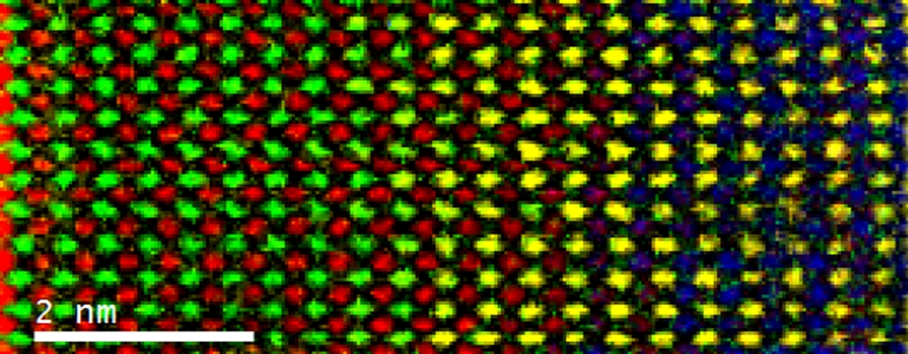
Fast atomic DualEELS color map across the SrTiO3/SrMnO4 interface
Paolo Longo, Ph.D., Gatan, Inc.
Sample courtesy of Professor David J. Smith at Arizona State University, Tempe, AZ
Microscope courtesy of Professor Ray Carpenter at Arizona State University, Tempe, AZ
Acknowledgement to Dr. Toshiro Aoki at Jeol USA (now at ASU) for helping set up microscope for experiment.
Legend
Red: Ti L at 456 eV; green: Sr L at 1940 eV; yellow: La M at 832 eV; blue: Mn L at 640 eV
Methods
Probe-corrected Jeol ARM 200 TEM/STEM microscope; S-FEG emission gun; Enfinium™ ER system; voltage: 200 kV; STEM mode; EELS low core-loss spectrum (280 – 2280 eV): 4 ms
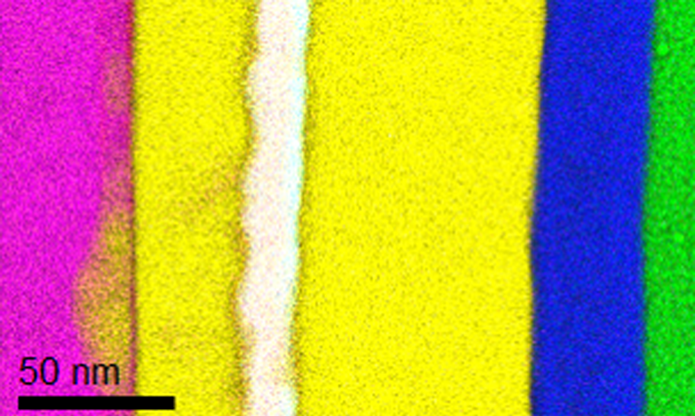
Fast DualEELS color map of a AuGeNi metal alloy ohmic contact for the fabrication of III-V transistor device structures; absolute compositional analysis also carried out
Paolo Longo, Ph.D., Gatan, Inc.
Sample courtesy of University of Glasgow
Microscope courtesy of Professor Ray Carpente at Arizona State University, Tempe, AZ
Acknowledgement to Dr. Toshiro Aoki at Jeol USA (now at ASU) for helping set up microscope for experiment.
AuGeNi ohmic contacts are widely used as they show a low contact resistivity and are typically compatible with the fabrication of III-V MOSFET devices1. However, they have the drawback of poor uniformity due to diffusion of the Au into the III-V substrate. This diffusion is dependent on temperature used during the annealing process after deposition of Au, Ge and Ni. It is clear that the performance of this type of contact will be influenced by both the material present and degree of roughness at the interface with the III-V substrate.
Fast DualEELS color map of a III-V transistor device structure before gate metallization process
Paolo Longo, Ph.D., Gatan, Inc.
Sample courtesy of University of Glasgow
Microscopecourtesy of Professor Gerald Kothleitner, TU-Graz, Austria
Pages
