付加製造(Additive Manufacturing)
一般的な課題
付加製造は、3Dプリンティングとも呼ばれ、複雑な形状、軽量構造、カスタマイズされた部品の製造を可能にし産業界に革命をもたらしています。また、航空宇宙、医療、自動車、消費者分野などでの採用が進むにつれ、性能、信頼性、スケーラビリティの向上が求められています。
これらの要求を満たすため、研究者や技術者は、材料の一貫性、機械的な完全性、表面の仕上げ、残留応力といった重要な課題に対応しなくてはなりません。これらの性能は、微細構造の変化、熱勾配、相変態、造形方向といった基本的な要因に影響されます。
そのため、プロセスにおけるパラメータと材料特性の関係を理解する事が不可欠であり、結晶粒構造、空隙率、元素分布といった特徴を評価することで、付加製造プロセスが最終部品の強度、耐久性、機能性にどのように影響するかについての重要な知見が得られます。
革新的な技術
付加製造プロセスにより製造された材料における重要な材料特性の関係をよりよく評価・理解するために、下記のような技術が利用可能です。.
|
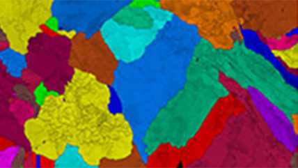
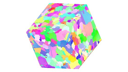
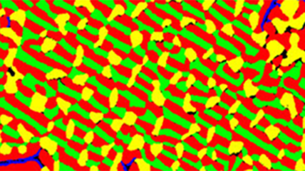
結晶の方位、相、粒界をマッピングすることで詳細な微細構造解析が可能になり、研究者がマイクロスケールでの材料特性、変形、破損のメカニズムを理解するのに役立ちます。 |
試料から発生する特性 X 線を検出することで、迅速かつ信頼性の高い元素分析を容易にし、研究者がさまざまな材料の主成分元素や微量元素を識別して定量化できるようにします。 |
|
元素組成と化学結合に関する原子レベルの知見を提供し、材料特性のより深い理解を通じて基礎研究と発見を前進させます。エネルギーフィルターTEM(EFTEM)も搭載。EELS.infoでEELSをさらに進化させましょう。 |
生物試料および無機試料の高解像度な視覚化を実現し、研究者が超微細構造、材料の成長、および破損のメカニズムを非常に明瞭に研究できるようにします。 |
|
制御された刺激の下でリアルタイムのナノスケールのダイナミクスを捉え、基礎的なメカニズムを明らかにして科学的発見を加速します。制御された刺激下におけるリアルタイムのナノスケールダイナミクスを捉え、基礎的なメカニズムを解明し、科学的発見を加速する。 |
インテグレーションSEM EDS、EBSD、CL、BSE、WDS を1つのプラットフォームに統合し、ワークフローを合理化し、複雑な材料への理解を深める包括的で高解像度の分析情報を提供します。 |
|
高解像度の非破壊元素分析が可能で、多層構造、センシティブまたは不定形な試料に最適です。 |
|
リソース
|
|
|
|
|
|
|
|