Energy dispersive x-ray spectroscopy (EDS/EDX) is an analytical technique employed for the elemental characterization of materials. By measuring the energy and intensity of x-rays emitted from a sample when exposed to an electron beam, this method reveals the intricate distribution of major, minor, and trace concentrations of most elements from the periodic table. EDS is not just a tool; it is a gateway to deeper understanding and discovery, providing invaluable insights into the significance of these elements. Its impact resonates across diverse fields, including microelectronics, catalysis, metallurgy, environmental science, and biomedical research, empowering us to unlock the mysteries of materials and innovate for a brighter future.
What is EDS/EDX? Advantages Workflow for EDS/EDX
What is EDS/EDX?
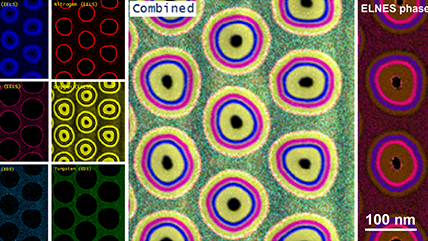
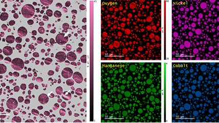
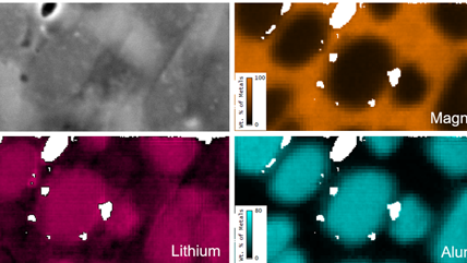
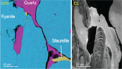
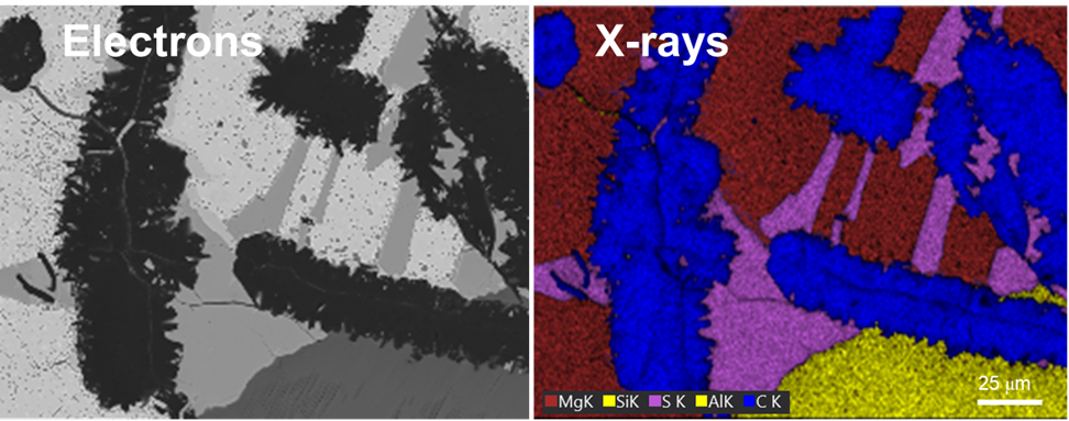
Together with other scanning electron microscopy (SEM) or transmission electron microscopy (TEM) techniques, EDS creates detailed elemental maps to enhance our understanding of a sample's surface properties.
The method relies on the concept that atoms have electrons organized in specific energy levels (or shells). When a sample is struck by a stream of high-energy electrons, the electrons in the target atoms are ejected from their inner shell, creating an electron vacancy. Following this, the electrons from the higher energy levels move down to fill the inner shell, releasing energy as x-rays in the process.
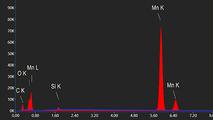
Depending on the shells that participate in the transition, a distinct x-ray is emitted. Every element in the periodic table possesses a unique electronic structure, resulting in varying energy levels. Consequently, the x-rays produced are specific to each element. By analyzing the energy and intensity of the characteristic x-ray emissions from each element, one can gather details about the elemental makeup of a sample.
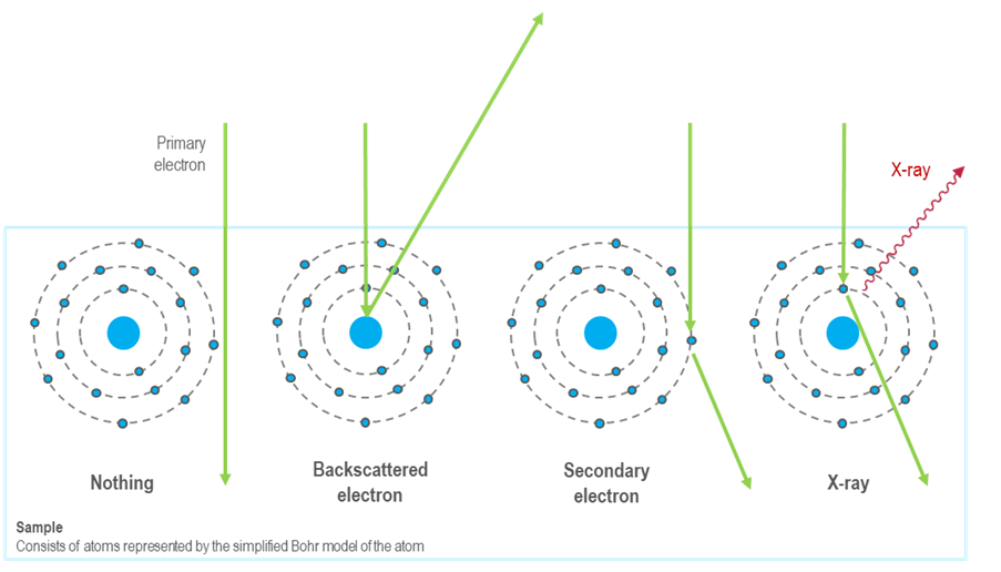
Silicon drift detectors (SDDs) are used to detect x-rays emitted from a sample. They convert these x-rays into electrical signals, which are then analyzed by a pulse processor and specialized software to generate an energy spectrum. This spectrum displays peaks that correspond to the energies of the characteristic x-rays produced by the sample. These peaks are then matched to specific elements using a spectral library. Analytical models have been developed to identify and quantify the elements present in a sample based on the characteristic x-rays detected.
Advantages of EDS/EDX
| Capability | Advantage |
|---|---|
| Reliably quantifies the composition of heavy elements | Its user-friendly nature is ideal for routinely collecting quantitative data about the elemental composition, including major, minor, trace elements, and impurities. |
| Non-destructive sample analysis | Accurately detects the characteristic x-rays emitted by the sample during electron beam excitation, without causing any permanent damage or altering its composition. |
| Shortens your time to results | The go-to method for rapidly identifying and quantifying elements within a sample for real-time analysis and decision-making. It is particularly suitable for high-throughput applications and routine analysis where time efficiency is paramount. |
| Sample versatility | Compatible with various bulk sample types, including solids, powders, and thin films. |
| Integrates with other SEM and TEM techniques | Offers the opportunity for simultaneous imaging and elemental analysis, which provides valuable insights into the chemical composition. This combination enhances our understanding and context for the materials being studied. |
Workflow for EDS/EDX
|
|
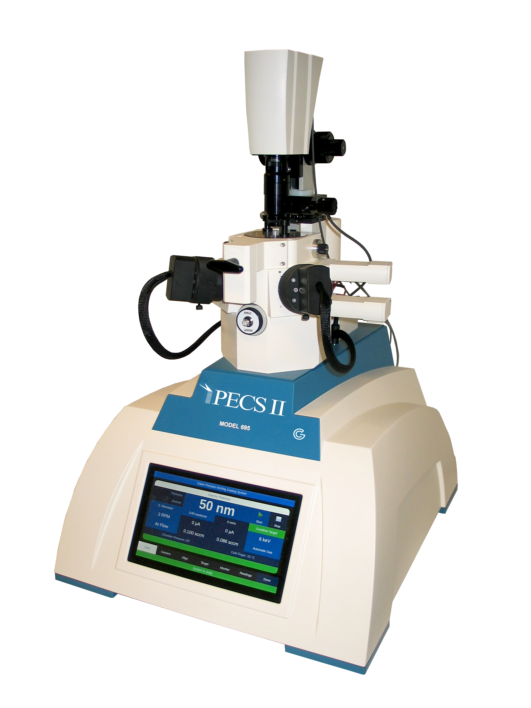
Step 1: Sample preparation Samples must be flat, polished, and mounted on holders or stubs. Non-conductive samples require a coating to eliminate charging effects that could cause image distortion or drift. The best way to accomplish this is to utilize a fully automated argon ion polishing system, like the PECS™ II instrument. A PECS II instrument can produce damage-free surfaces, cross-sections, and deposit coatings to protect or eliminate charging. |
|
|
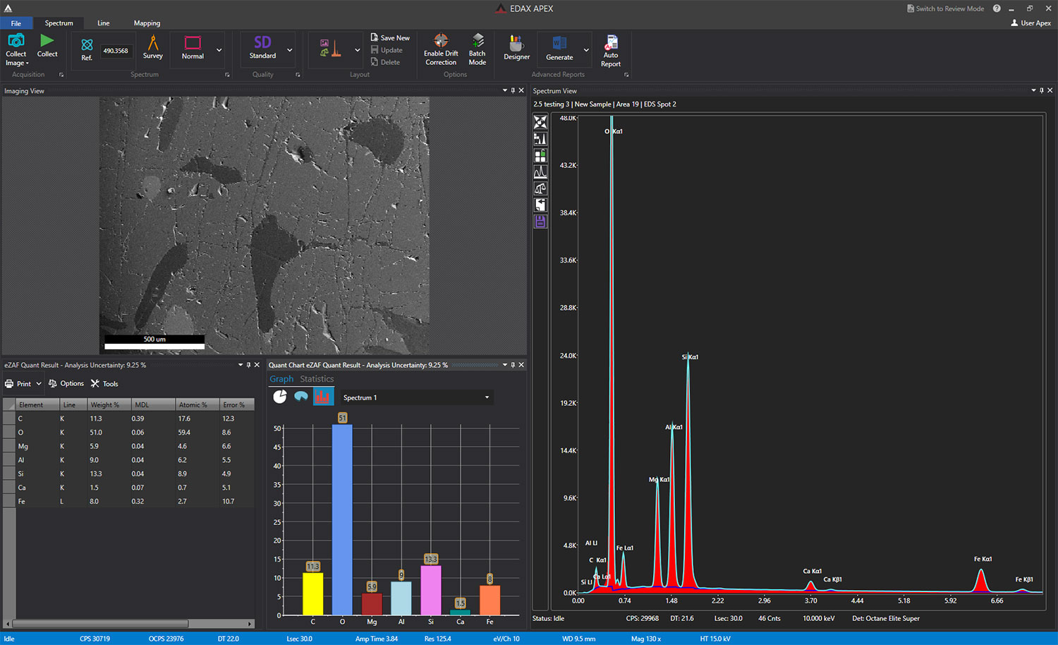
Step 2: Data collection EDS detectors collect emitted x-rays when the microscope beam hits the sample. These x-rays and their intensities are then converted into the concentrations of the various elements in the sample. The EDAX APEX and DigitalMicrograph software enable this conversion. EDS can also be combined with related techniques, such as electron backscatter diffraction (EBSD) or wavelength dispersive x-ray spectroscopy (WDS) in the SEM, or energy electron loss spectroscopy (EELS) or 4D STEM in the S/TEM, to provide a further understanding of the material’s composition. Visit gatan.com or edax.com for more information on EDS data collection.
|
|
|
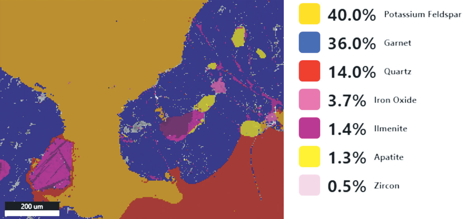
Step 3: Analyze Once the data is collected, it can be used to produce elemental maps, distributions, phase maps, and quantification analysis. This information can tell you more about the sample’s chemical makeup. All of this can be performed directly in the EDAX APEX and DigitalMicrograph software platforms. Visit gatan.com or edax.com for more information on EDS analysis software. |


DigitalMicrograph, also known as Gatan Microscopy Suite, drives your digital cameras and surrounding components to support key applications including tomography, in-situ, spectrum and diffraction imaging, plus more.

A powerful tool that expands the utility of your Gatan camera to address 4D STEM diffraction studies.


Preserve sample integrity with controlled transfer from an inert environment to the TEM.


Quantify microstructural changes in materials due to applied mechanical loading.


Digital beam control and image processing to enhance the photographic quality of your digital images.

A powerful method of obtaining detailed analytic data from a sample on an electron microscope equipped with scanning mode.

The most intuitive and easy-to-use energy dispersive spectroscopy (EDS) tool for scanning transmission electron microscope (STEM) applications and in-situ microscopy.


The revolutionary energy dispersive x-ray spectroscopy (EDS) system for compositional analysis in the scanning electron microscope (SEM).

Premier software program for collecting and analyzing energy dispersive spectroscopy (EDS) data and the compositional characterization of materials.
 System")
Combines the latest advances in energy dispersive spectroscopy (EDS), electron backscatter diffraction (EBSD), and wavelength dispersive spectrometry (WDS) in a single analytical tool.
 System")
A world-class materials characterization solution that provides users with elemental composition and crystallographic orientation results in one easy-to-use package.
 System")
By integrating energy dispersive spectroscopy (EDS) and wavelength dispersive spectrometry (WDS) analytical techniques on a single platform, EDAX Neptune provides the power and flexibility of EDS with the resolution, precision, and detection limits of WDS.

Combines the EDAX wavelength dispersive spectrometry (WDS) analysis software with state-of-the-art spectrometers for improved accuracy and precision, guaranteeing the best results for your materials analysis.

The game-changing advancements in the Octane Elite silicon drift detectors (SDDs) take energy dispersive spectroscopy (EDS) analysis to the next level.

An enhanced energy dispersive spectroscopy (EDS) platform with the latest silicon drift detector (SDD) technology and high-speed electronics advancements.

Delivers powerful energy dispersive spectroscopy (EDS) analytical capability in a compact package, maximizing performance and flexibility while providing streamlined operation to guarantee fast results and ease of use.

The first and only system that quantitatively reveals the distribution of lithium in scanning electron microscopes