Electron backscatter diffraction (EBSD) provides crystallographic orientation and phase information necessary to understand materials' microstructure-property relationships.
What is EBSD?
Developing and optimizing materials, as well as increasing their accessibility and affordability, is crucial for technological and economic progress. Materials scientists study the interplay between a material's processing, the internal microstructure that develops, and the resulting critical properties to optimize its performance for any given application. Material characterization lies at the heart of these studies, and electron microscopy characterization is often the best tool for atomic-to-mesoscale analysis.
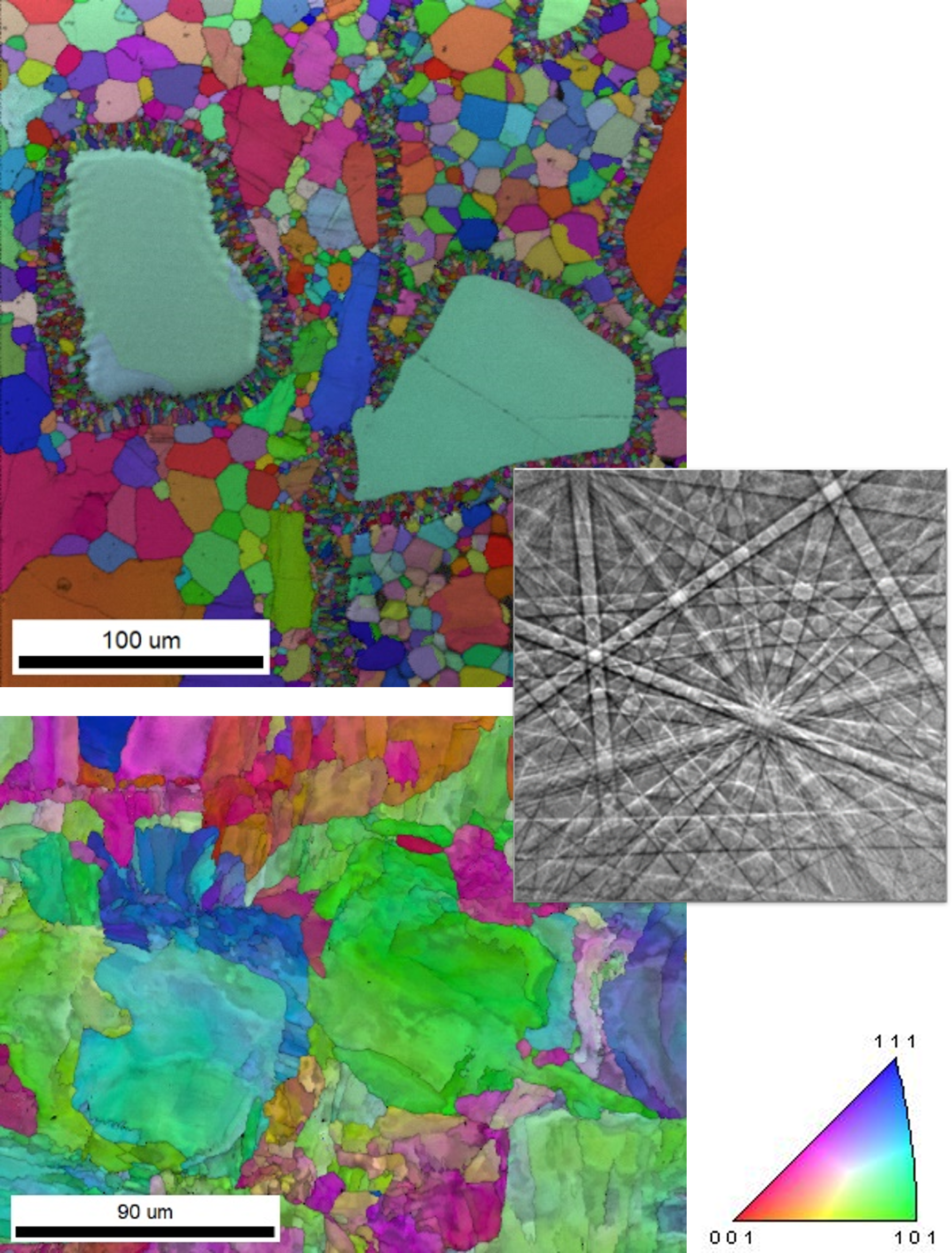
EBSD is an important tool for characterizing the crystallographic microstructure in materials and earth sciences. This technique involves using a scanning electron microscope (SEM) to collect statistical data on grain size, crystal orientation, grain boundaries, and texture, which are critical parameters in determining the material properties of crystalline materials. Understanding the relationship between microstructure and properties allows scientists and engineers to develop superior performing, lighter, stronger, and faster materials for various applications such as structural metals, ceramics, energy materials, semiconductors, automobiles, aerospace, and additive manufacturing. EBSD is also valuable for gaining insights into the properties of geological samples that have a crystalline structure, including shells, fossils, meteorites, rocks, and minerals. In some cases, EBSD is the only technique capable of analyzing these delicate samples.
EBSD is a SEM-based technique that measures orientations accurately and rapidly at the microscopic scale. EBSD patterns are obtained by focusing a stationary electron beam on a tilted (~ 70°) crystalline sample. The resulting diffraction pattern is captured on a phosphor screen (e.g., EDAX Velocity™ detectors) or with a direct detection sensor (e.g., EDAX Clarity™ detectors). The bands in the pattern represent the geometric projections of the diffracting planes within the crystal. The geometric arrangement of these bands is analyzed to determine the orientation and phase from each EBSD pattern. Once the operator defines the area of interest and sampling step size, the system automatically performs the orientation measurements. These measurements yield a wealth of information that can be visualized through different maps, plots, and charts. EBSD can also be combined with different techniques, such as energy dispersive x-ray spectroscopy (EDS), to gather information about a material's chemical composition and provide users with a more comprehensive understanding of the material.
Visit EDAX.com for more information on EBSD products and applications.

Advantages of EBSD
EBSD enables rapid characterization of crystalline microstructures on a nano-to-mesoscale, offering unique advantages for researchers to understand the processing-microstructure-property relationship in various materials.
| Capability | Advantage |
|---|---|
| Rapidly and accurately measures crystal orientations | Visualizes and quantitatively describes material microstructures with statistical significance |
| Determines the texture, or preferred orientation, of a material | Identifies if specific orientations occur significantly more often than a random distribution, which can affect material properties |
| Measures the strain within a deformed material | See the actual deformation gradients within a microstructure rather than relying on an average strain value |
| Identifies and measures phases | Determines the actual phases by using EBSD with EDS for complete phase characterization |
| Pinpoints grain boundaries in a microstructure | Distinguishes specific grain boundaries, including twin boundaries and phase transformations, within a microstructure |
| Measures grain size | Quickly determines a common single number used to describe the microstructure |
Workflow
|
|
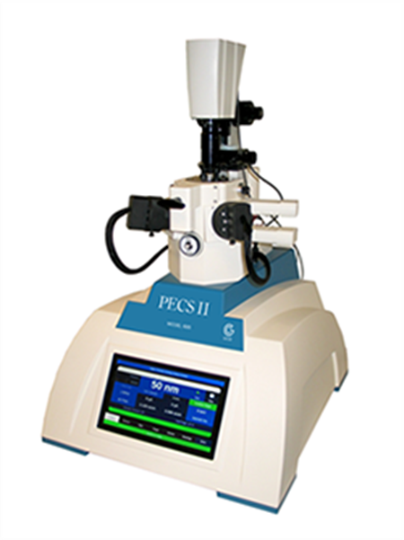
Step 1: Sample preparation It is important to carefully prepare samples for EBSD applications because the technique requires a very smooth specimen surface to avoid shadows on the diffraction pattern. The best way to accomplish this is to utilize a fully automated argon ion polishing system, like the PECS™ II instrument. A PECS II instrument can produce damage-free surfaces, cross-sections, and deposit coatings to protect or eliminate charging. |
|
|
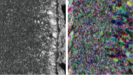
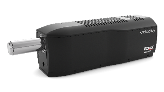
Step 2: Data collection EBSD systems collect maps by capturing EBSD diffraction patterns from a specific area of the sample defined by the user. These patterns are then indexed to determine the local crystal structure and orientation. EBSD can also be used in conjunction with related techniques, such as EDS, to gain a deep understanding of the material's composition. Visit EDAX.com for more information on EBSD data collection. |
|
|
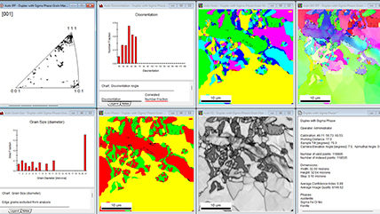
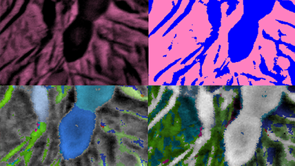
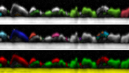
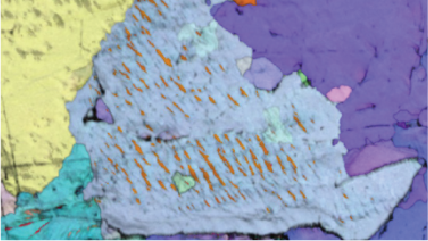
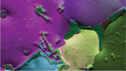
Step 3: Analyze EBSD can utilize various powerful post-processing analysis techniques. EDAX OIM Analysis™ is the premier microstructural visualization and analysis tool for interrogating and understanding electron EBSD mapping data. EBSD maps can be generated from raw data to provide details about orientation, phase distribution, grain size and shape, grain boundary structure, and local deformation of crystallographic microstructures. This information helps users visualize, characterize, understand, and communicate the details of their material's microstructure. Visit EDAX.com for more information on EBSD analysis software. |


DigitalMicrograph, also known as Gatan Microscopy Suite, drives your digital cameras and surrounding components to support key applications including tomography, in-situ, spectrum and diffraction imaging, plus more.

Designed to produce consistent, high-quality surfaces across semiconductors, batteries, and advanced materials using a single, integrated workflow.

Designed to deliver consistent, high‑quality cross‑section milling for a broad range of materials found in industrial laboratory environments.

The premier microstructural visualization and analysis tool for interrogating and understanding electron backscatter diffraction (EBSD) mapping data.

Enables the characterization of electron backscatter diffraction (EBSD) patterns within the user-friendly APEX software platform.
 System")
Combines the latest advances in energy dispersive spectroscopy (EDS), electron backscatter diffraction (EBSD), and wavelength dispersive spectrometry (WDS) in a single analytical tool.
 System")
A world-class materials characterization solution that provides users with elemental composition and crystallographic orientation results in one easy-to-use package.

Offers high-speed electron backscatter diffraction (EBSD) mapping with the best indexing performance on real-world materials.

The world’s first commercially available electron backscatter diffraction (EBSD) detector with unparalleled performance as low as 3 kV.