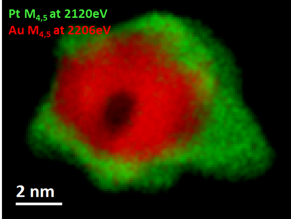
EELS color map of a Pt/Au catalyst nanoparticle
Paolo Longo, Ph.D., Gatan, Inc.
Sample courtesy of Professor Gianluigi Botton at CCEM, Hamilton, ON, Canada
Microscope courtesy of CCEM, Hamilton, ON, Canada
Acknowledgement to Dr. Andreas Korinek at CCEM for helping set up microscope for experiment.
EELS data taken using a probe and image-corrected FEI Titan TEM/STEM microscope equipped with X-FEG emission gun and a fully loaded GIF Quantum® ERS system. Au M4,5-edges at 2206 eV (red) and Pt M4,5-edges at 2206 eV (red).
Methods
Voltage: 200 kV; data taken in STEM mode; EELS core-loss spectrum (1400 – 3400 eV) exposure time: 20 ms; convergence angle: 19 mrad; collection angle: 34 mrad; beam current: 180 pA; total exposure time: <5 min
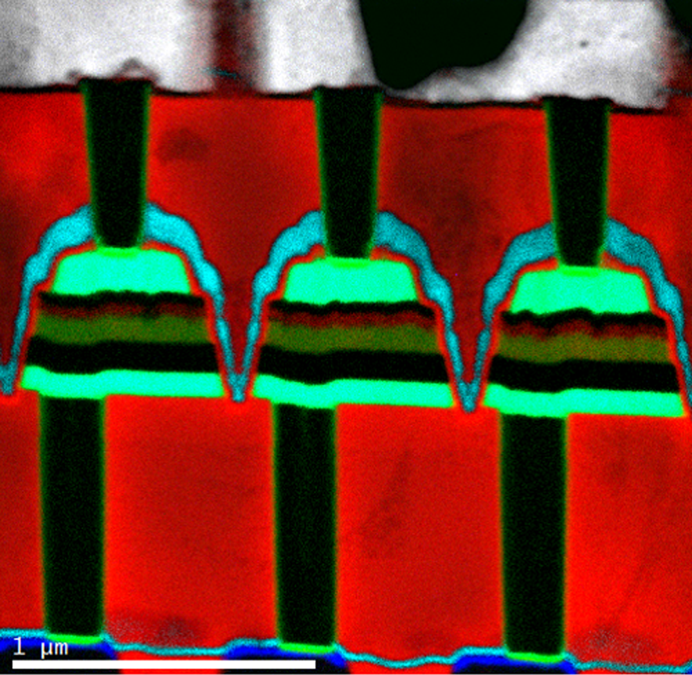
EELS color map of a magnetic device
Paolo Longo, Ph.D., Gatan, Inc.
Legend
Cu L at 931 eV (grey); O K at 532 eV (red); N K at 401 eV (light blue); Ti L at 456 eV (green); Co L at 779 eV (blue)
EELS color map of a Pd/Au catalyst particle
Paolo Longo, Ph.D., Gatan, Inc.
Sample courtesy of Professor Jianfang’s group, Chinese University, Hong Kong
Microscope courtesy of IBM, Fishkill, NY
Pd/Au alloys have attracted a lot of interest due to their resistance at high temperatures, and this explains their use in several fields, such as CO and hydrocarbon oxidation, synthesis of vinyl acetate monomer, hydrocarbon hydrogenation, and many others. Pd is the catalytic center, whereas the Au has the effect of changing the chemical properties at the surface of the Pd-Au alloy. This change influences the catalytic properties. Hence, the study of the chemistry and the elemental distribution is important to understand the properties of the whole catalyst system.
Pages


