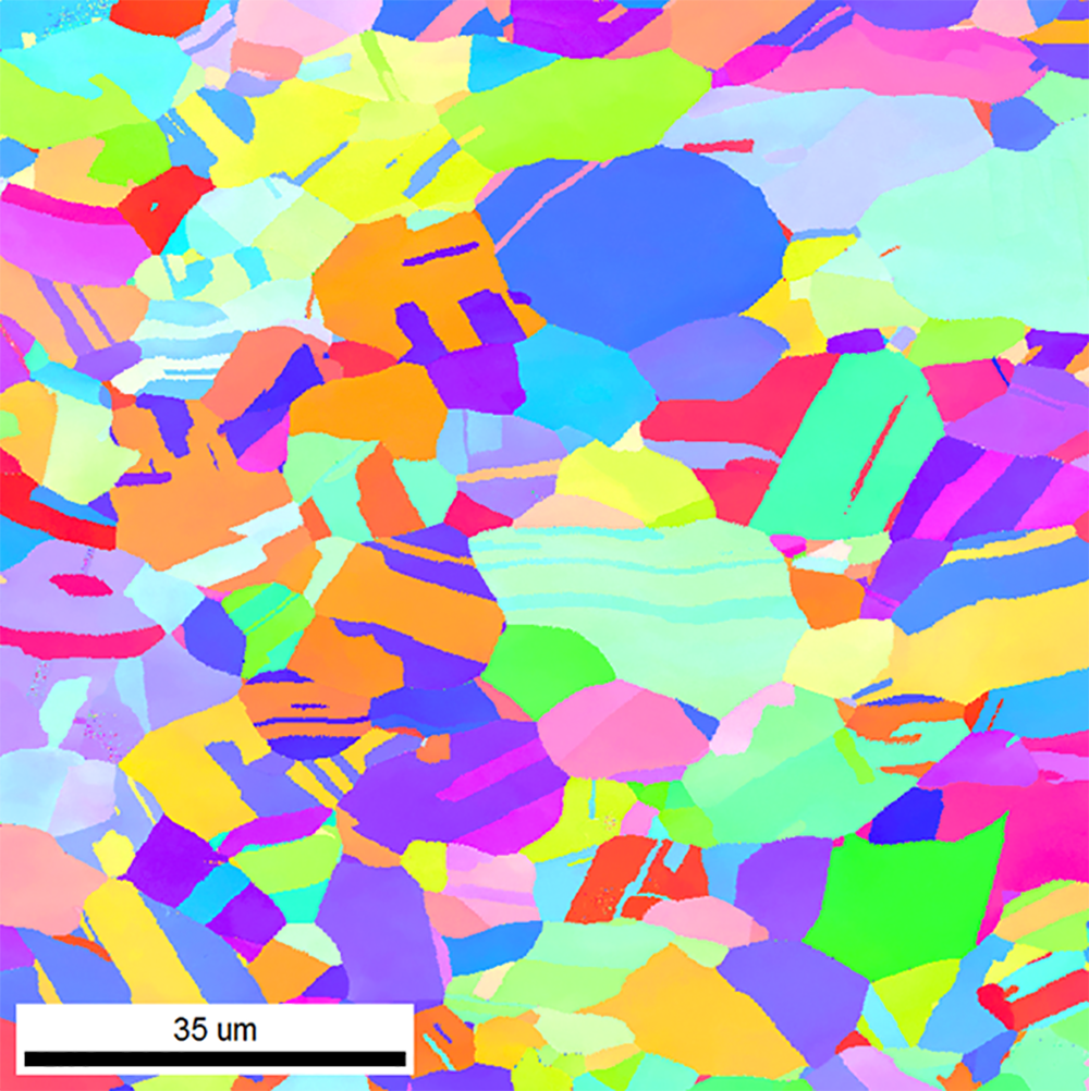
EBSD inverse pole figure map of copper sample
Data courtesy of Evans Analytical Group, Sunnyvale, CA
Through silicon via
Data courtesy of the Fraunhofer Institute, Dresden, Germany (© 2013 Fraunhofer IZM, Dept. HDI&WLP/ASSID).
Backscattered electron image of 2.5 interposer structure prepared with Ilion II system.
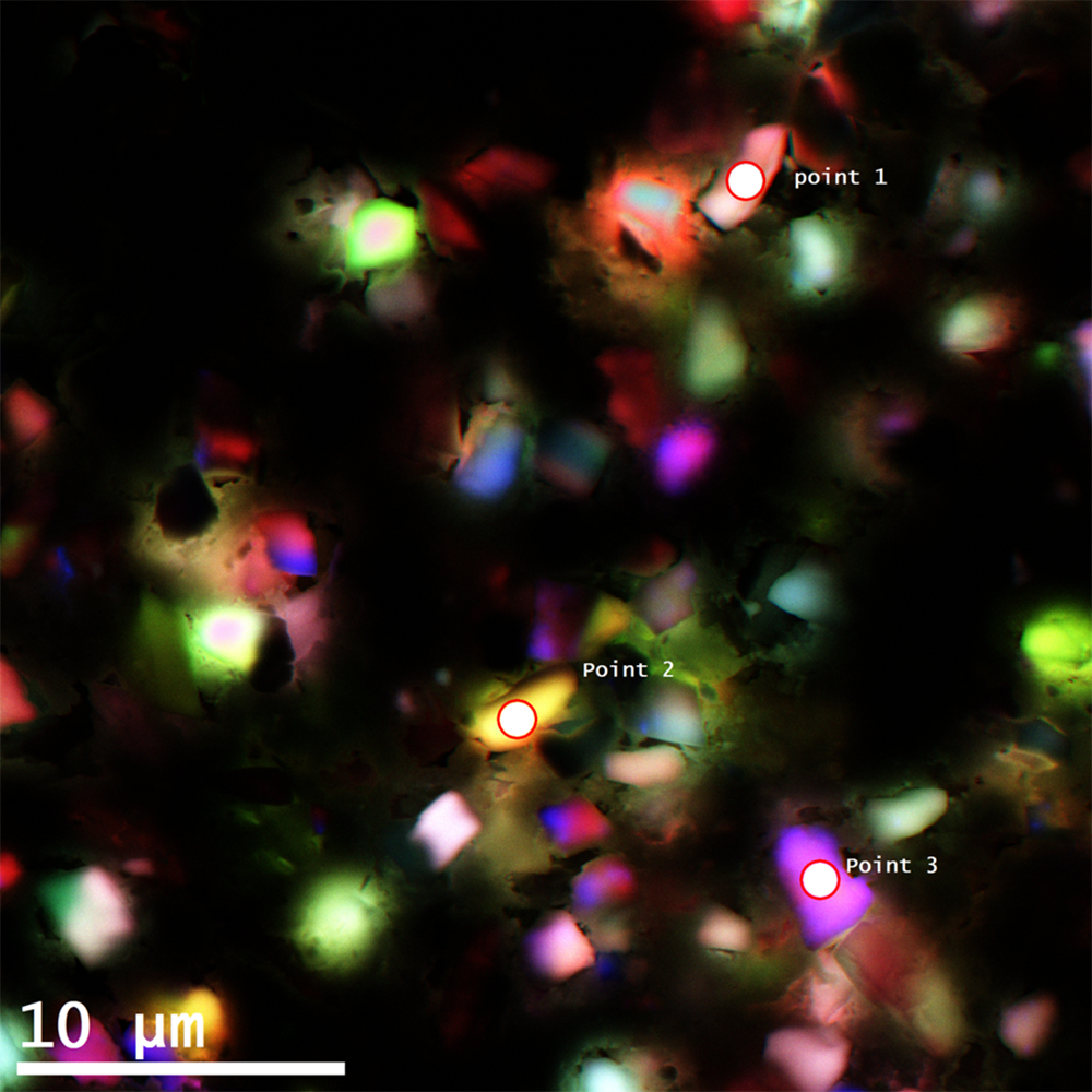
Cathodoluminescence image of paint pigment
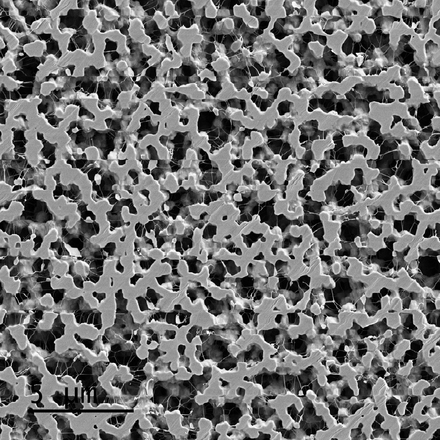
Data courtesy of Prof. Nicholas Leventis, Chemistry Department, Missouri University of Science and Technology
Cathodoluminescence image of paint pigment sample prepared with Ilion II and imaged with MonoCL4™ system.
Polymer aerogel
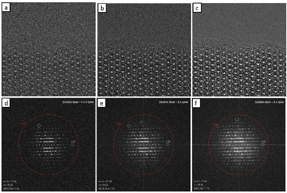
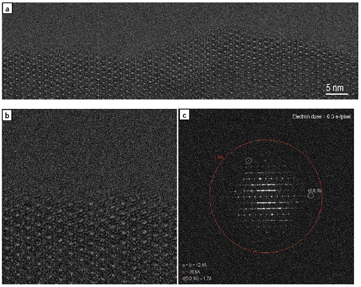
Zeolite beta low dose image series
Sample courtesy of Prof. D.L. Zhang at Jilin University, China.
(a) – (c) Zeolite beta electron dose series of 0.5, 2, and 8 e-/pixel; (d) – (f) corresponding FFT images. As dose increases image quality improves and more reflections can be seen in the FFT image.
Zeolite beta low dose images
Sample courtesy of Prof. D.L. Zhang at Jilin University, China.
(a) A single sub-image frame (0.125 s exposure) of zeolite beta along [100] zone axis. Electron dose for this image is 0.5 e-/pixel or 11 e-/A2; (b) Enlarged area of the outlined in (a); (c) FFT image of (b). The d-spacing of (0, 0, 16) is 1.7 A.
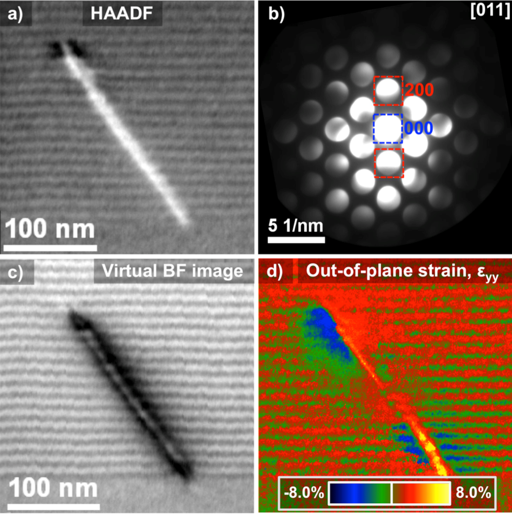
Nano-beam electron diffraction full 2D strain mapping
Data courtesy V. B. Ozdol et al., National Center for Electron Microscopy, Lawrence Berkeley National Laboratory and Department of Materials Science and Engineering, University of California, Berkeley, California.
a) HAADF image of a GaAs/GaAsP multilayer laminate; b) Integrated diffraction pattern of the superlattice structure along the [011] zone axis; c) Virtual BF image extracted from 4D data cube quantifying strain down to 1.2 nm resolution in full 2D area in eyy; d) exx strain for same area shown.
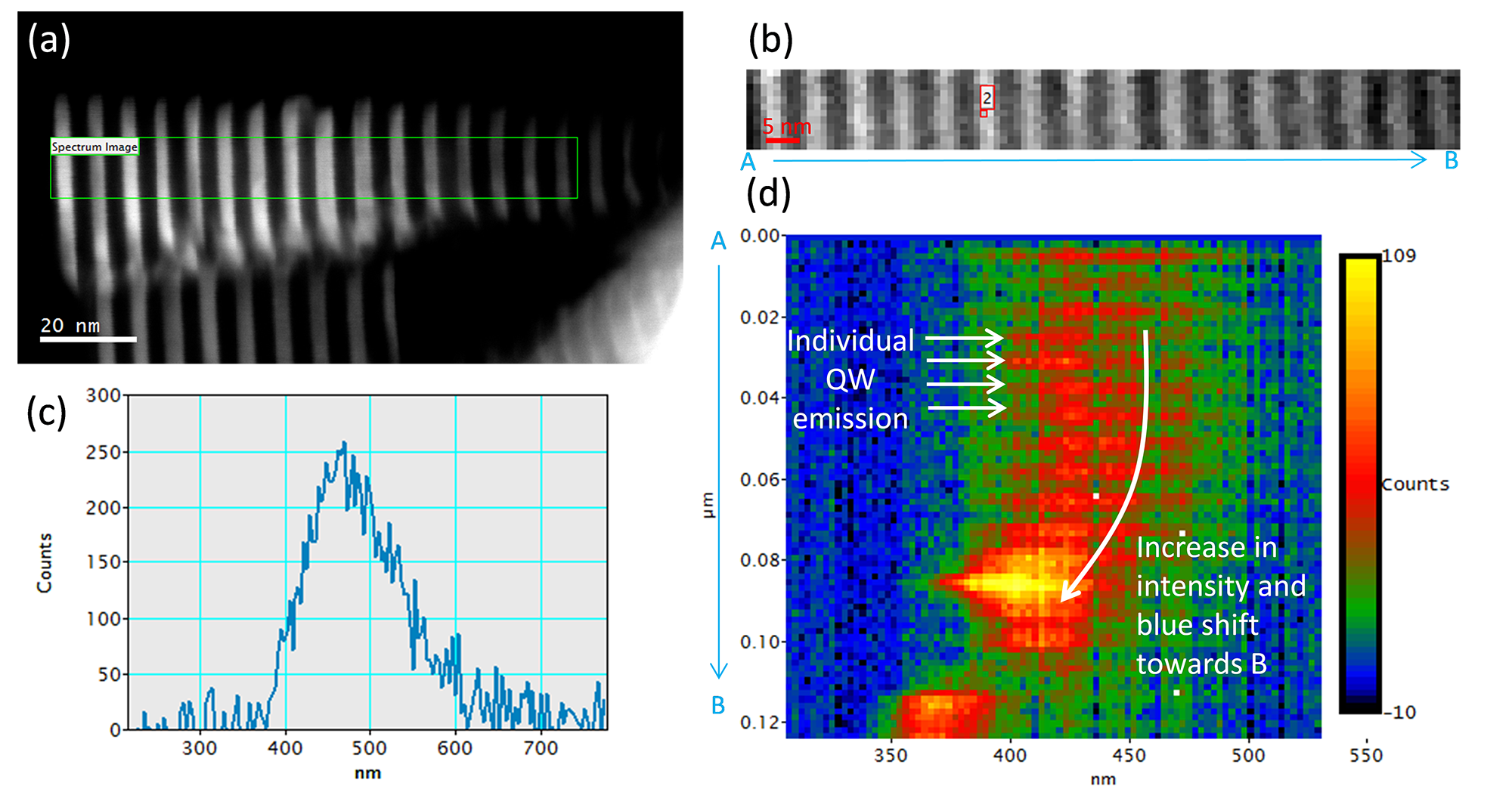
Correlating microstructure with luminescence properties at the nanoscale
Data courtesy of Dr. R. Williams, Ohio State University
Cathodoluminescence analysis of a GaN/AlN nanowire in STEM (a) Dark field STEM image, (b) cathodoluminescence spectrum-image acquired from the region indicated by the green rectangle in (a), (c) A cathodoluminescence spectrum extracted from the spectrum-image, and (d) a projection of the cathodoluminescence spectrum with the information along the y-axis (radial direction) of the nanowire summed into a single value. The resultant data set shows the spectral information as a function of position along the nanowire length.
Dislocation density analysis in semiconductors
Panchromatic cathodoluminescence image of bulk GaN sample. Dark spots (some indicated by blue arrows) correspond to threading dislocations. A dislocation density of 5 x 105 cm-2 was measured. Acquisition time = 30 s. The corresponding secondary electron image (revealing topography) showed no contrast.
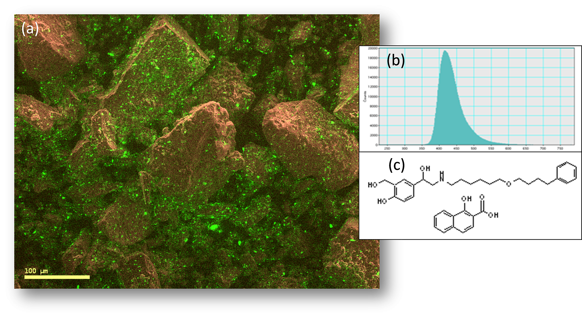
Revealing the distribution of organic materials in the SEM
Data courtesy of G Nichols, Pfizer UK
Distribution of drug within a pharmaceutical pill. Composite color image showing the spatial distribution of the micronized drug, salmeterol xinafoate. The cathodoluminescence image acquired at 415 m showing the drug is displayed in green and the secondary electron image reveals the non-cathodoluminescent lactose monohydrate (shown in brown).
Pages
