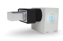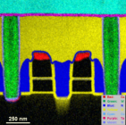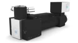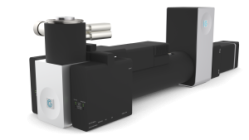
NUANCE mission is to provide and continually update state-of-the-art and core analytical characterization instrumentation resources, with 24/7 open access, for the NU...
What is 4D STEM?
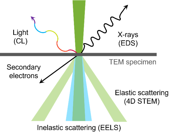
In scanning transmission electron microscopy (STEM), the electron beam is focused on an electron transparent specimen to make a probe from a few nanometers down to nearly atomic dimensions. Electrons interact with the specimen, and once they are scattered, different types of signals can be measured:
- X-rays (EDS)
- Back-scattered electrons
- Light (cathodoluminescence)
- Auger electrons
- Secondary electrons
- Inelastically scattered electrons (energy loss spectroscopy)
- Elastically scattered electrons (diffraction)
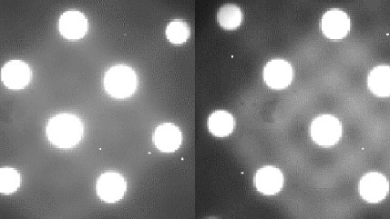
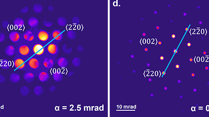
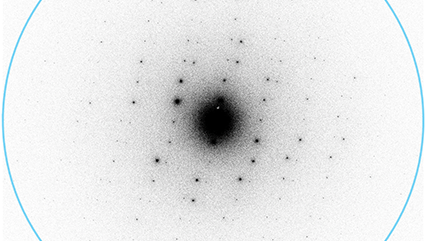
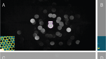
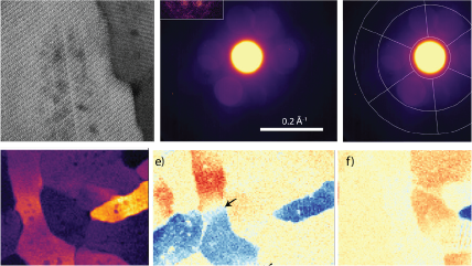
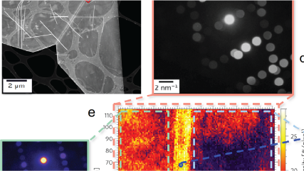
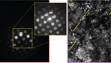
In four-dimensional (4D) STEM, the probe is rastered on the specimen in a two-dimensional (2D) array and at each probe position, a 2D diffraction pattern is imaged on a pixelated detector, thus generating a 4D data cube that can be further analyzed.
Video courtesy of Colin Ophus, Molecular FoundryNaming conventions
Several terms have been used in the literature referring to electron diffraction patterns produced using a converged (STEM) probe:
- Convergent beam electron diffraction (CBED)
- Microdiffraction
- Nanodiffraction
- Diffraction imaging
And some other terms in the literature that refer to a 4D STEM technique:
- Position resolved diffraction (PRD): Used in earlier works where a 2D scan was used instead of only a line scan
- Spatially resolved diffractometry: Highlighting virtual imaging application
- Momentum-resolved STEM: Another name for 4D STEM, because it allows for evaluation and combination of real- and momentum space information, simultaneously
- Scanning electron Nanodiffraction or nanobeam electron diffraction (NBED): Usually when a nanometer-scale beam is used
- Pixelated STEM
STEM detectors
Conventional STEM detectors usually have an annular geometry and record a single value per probe position:
- Bright-field (BF): Collects the intensities of the unscattered direct beam (collection angle < 10 mrads)
- Annular bright-field (ABF): Same as BF, but instead of using a full disk for detection, only the outer annulus of the bright-field disk is used giving unique contrast effects
- Annular dark-field (ADF): Collects the intensities of the scattered electrons (10 mrads < collection angle < 50 mrads)
- High-angle ADF (HAADF): Is commonly called Z-contrast imaging and collects the intensities of electrons scattered with a larger angle compared to those collected with ADF, thus minimizing the Bragg scattered electrons (collection angle > 50 mrads)
Note: Angles above are based on a 200 kV, non-corrected STEM and Individual set up values may vary.
Beyond single-value detectors, are classes of multi-value (more than one signal is detected per probe position) detectors. The simplest of these are quadrant detectors, but many other types of segmented detectors exist. These multi-value detectors are usually annular as well, have 4 to 16 segments, and are used for differential measurements (see differential phase-contrast section).
A generalized multi-value detector is the pixelated STEM detector (e.g., cameras). Availability of high-speed, high-sensitivity, and high-dynamic-range detectors (including direct electron detectors) along with advances and availability of computational power, enable large-scale 4D experiments in the recent years.
Uses for 4D STEM data
Below are a few examples of applications of 4D STEM in material science. However, we greatly encourage you to read Microscopy and Microanalysis 25, 563-582, 2019 for more examples and further details on each method.
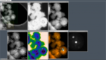
One of the main applications of 4D STEM diffraction is virtual imaging. This is done by generating:
- Virtual selected area diffraction image: Sum the diffraction images from multiple selected real space probe positions (pixels) in the 4D data cube
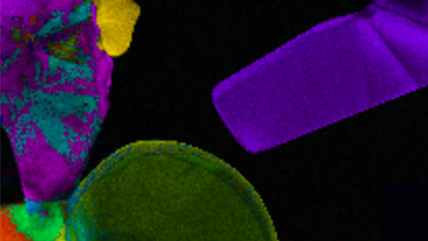
- Virtual bright/dark field image: Apply a certain math (sum, subtract, …) to the intensities of a subset of pixels in the diffraction domain and assigning the resulting value to the corresponding pixels in the virtual image
In comparison to conventional STEM imaging, virtual imaging:
- Allows for design and application of a variety of geometry and combination of STEM detectors that would be otherwise impossible to physically manufacture and use in a real microscope
- Removes the limitation of having to use a certain number of and the relative angular range of STEM detectors that can be used simultaneously during an experiment
- Produces images with a higher signal to noise ratio and is not as much affected by specimen bending and dynamical scattering (Ultramicroscopy 155, 1–10, 2015)
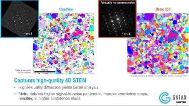
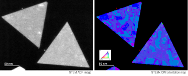
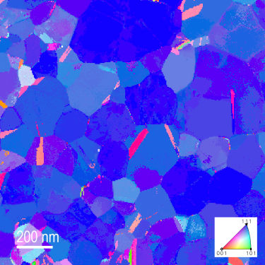
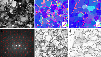
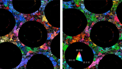
Like electron backscatter diffraction (EBSD) in a scanning electron microscope (SEM), orientation mapping at higher resolution is possible in a TEM using 4D STEM. This can be done in two ways:
- Fitting Kikuchi diffraction patterns: Better for thicker specimens but can fail in regions with high local deformation
- Diffraction spot indexing: Preferred for thinner specimens, and uses a template matching method (can be automated)
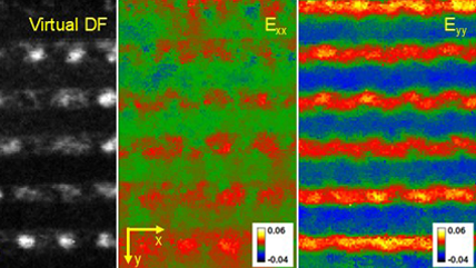
Mechanical and electrical properties of materials are directly related to the variations in their local atomic spacings (strain). For an overview and comparison of different strain mapping methods in a TEM we recommend reading MRS Bulletin, 39, 138-146, 2014. Using 4D STEM specifically, there are two ways to measure strain:
- CBED: Higher-order Laue zone (HOLZ) features are carefully measured; this method requires rotating the sample into a certain orientation and has limitations on the range of the specimen thickness
- NBED: Inverse relationship between atomic distances and diffraction spots is used
Strain mapping using NBED does not rely on a field of view with a single well-aligned zone axis, but requires a balance/optimization between the real space and reciprocal space resolution:
- Larger convergence angle (smaller STEM probe): Improves the spatial resolution, but reduces the strain measurement precision
- Smaller convergence angle (larger STEM probe): Improves the strain measurement precision but at a lower spatial resolution
Note: In addition to the convergence angle, the application of precession electron diffraction (PED) can enhance the precision of the strain measurements by minimizing the heterogeneity in the diffraction disks.
4D STEM strain measurements are not only limited to crystalline materials, and can also be applied to amorphous and semi-crystallin materials (Applied Physics Letters, 112, 171905, 2018).
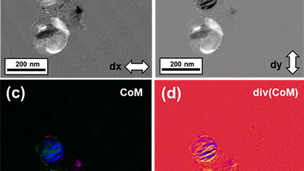
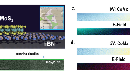
Fixed segmented STEM detectors have been used to measure the deflection of the electron beam and correlate it to the sample’s electric field (electrostatic potential gradient) for many years; one drawback of such detectors is the limitation of information transfer efficiency over several spatial frequencies (Optik, 54, 83-96, 1979). 4D STEM overcomes this limitation by measuring the movement of the center of mass (COM) of the bright field disk at each pixel position and calculating the electric field using the resulting COM displacement vector maps. Because DPC results in an image that is directly interpretable as the (projected) electrostatic potential of a thin specimen, it makes imaging low-z elements possible (unlike HAADF imaging or Z-contrast imaging that is great for elements with high scattering power).