Strain Mapping
The mechanical and electrical properties of materials are directly related to the variations in their atomic spacing (strain). In a transmission electron microscope (TEM), one can measure the crystal lattice deformation by comparing the interplanar distances (d) in the interest area to an unstrained reference region (for an overview, see MRS Bulletin, 39, 138-146, 2014).
Imaging methods (e.g., high-resolution TEM (HRTEM) or scanning TEM (HRSTEM)) measure the interplanar distances (d), and diffraction methods (e.g., nanobeam electron diffraction (NBED)) measure the reciprocal distances (g = 1/d).
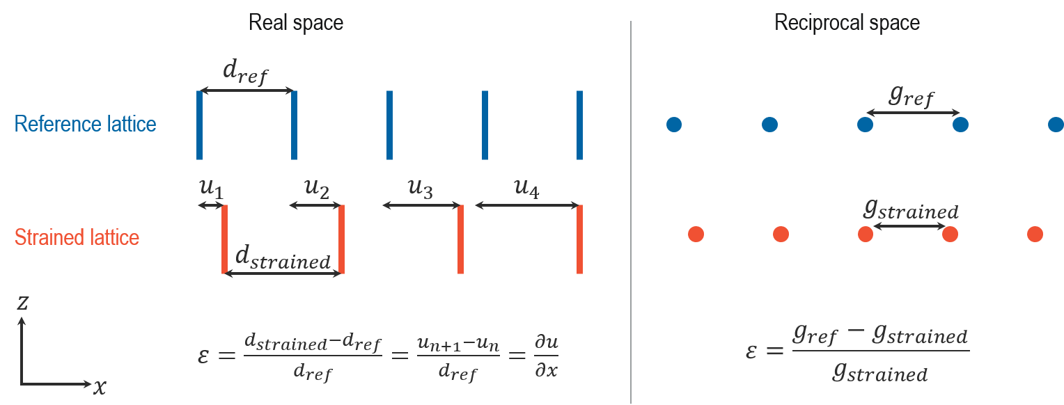
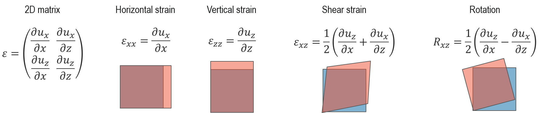
Both of these methods in the TEM provide 2D measurements of the crystal lattice deformation, which you can represent using a 2 x 2 matrix. You can then calculate the 2D strain maps, as shown below:
Using 4D STEM specifically, there are two ways to measure strain:
- CBED: Higher-order Laue zone (HOLZ) features are carefully measured; this method requires rotating the sample into a certain orientation and has limitations on the range of the specimen thickness
- NBED: Inverse relationship between atomic distances and diffraction spots is used
Strain mapping using NBED does not rely on a field of view with a single well-aligned zone axis but requires a balance/optimization between the real space and reciprocal space resolution:
- Larger convergence angle (smaller STEM probe): Improves the spatial resolution but reduces the strain measurement precision
- Smaller convergence angle (larger STEM probe): Improves the strain measurement precision but at a lower spatial resolution
Note: 4D STEM strain measurements are not limited to crystalline materials but can also be applied to amorphous and semi-crystalline materials (Applied Physics Letters, 112, 171905, 2018).
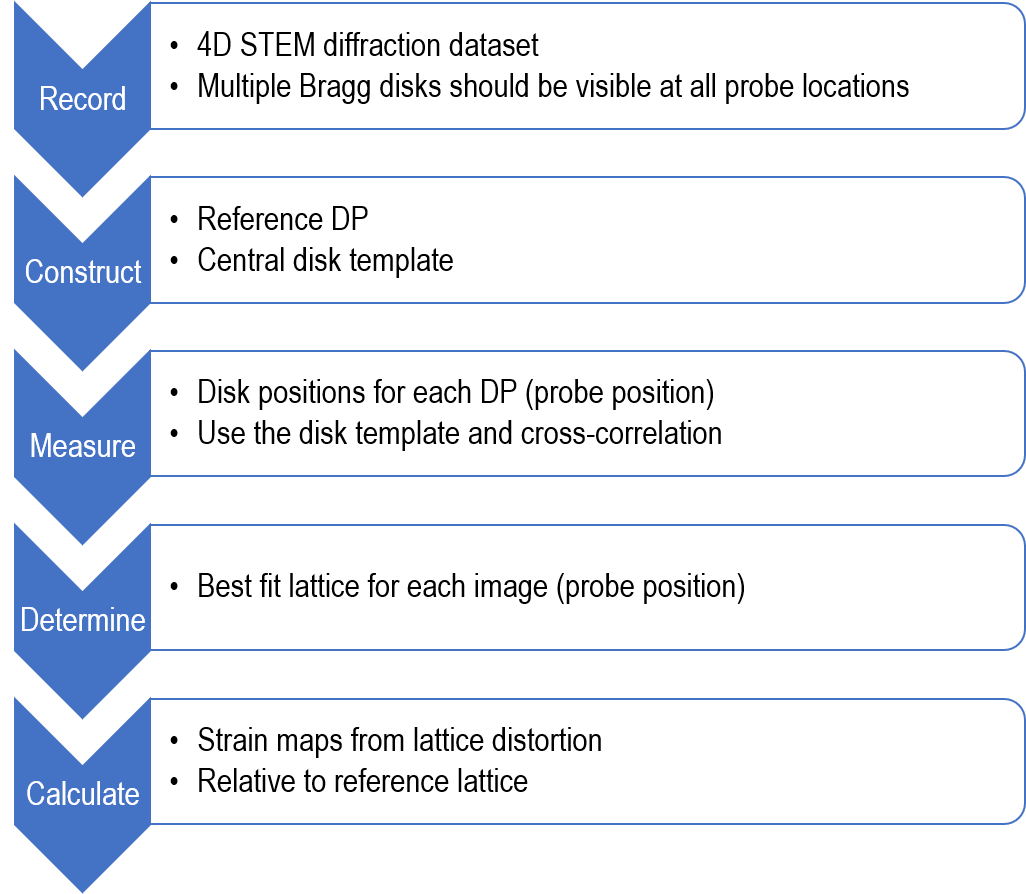
4D STEM Strain Mapping in DigitalMicrograph
STEMx® applies the same theory for strain measurements using NBED datasets in DigitalMicrograph® as shown in the flowchart below:
4D STEM data collection considerations for strain mapping
For the acquisition of 2D strain mapping data, the specimen and microscope setup are critical. This method depends on a 2D array of non-overlapping diffraction disks, with little contrast within the disks and sharp edges to the disks.
Convergence angle: The convergence angle (condenser aperture and lens configurations) determines the spatial resolution. A larger convergence angle produces a smaller STEM probe (better spatial resolution) and vice versa. On the other hand, the diameter of the diffraction disks directly relates to the convergence angle. A larger convergence angle gives larger disks, and depending on the d spacing, there is a higher chance of disk overlap (which should be avoided).
Camera length: Select a camera length that allows you to image the first 2 or 3 orders of diffraction disks on the camera. Remember that the larger camera length spreads the disks over a larger number of pixels (suitable for disk fitting algorithm) but results in less signal per camera pixel (bad for disk fitting algorithm). You should also consider this when selecting the convergence angle.
Specimen thickness and orientation: Choose a sample thickness thick enough so that there is a reasonable amount of scattering (without stress relaxation) but not so thick as to generate inelastic scattering (too much sub-structure in the diffraction disk and poor disk fitting).
Other considerations: Energy-filtered 4D STEM can reduce the inelastic scattering effects and greatly enhance strain mapping results.
Removing the inelastic scattering improves the contrast. All the lines and features in the diffraction pattern are now visible.
Strain calculations
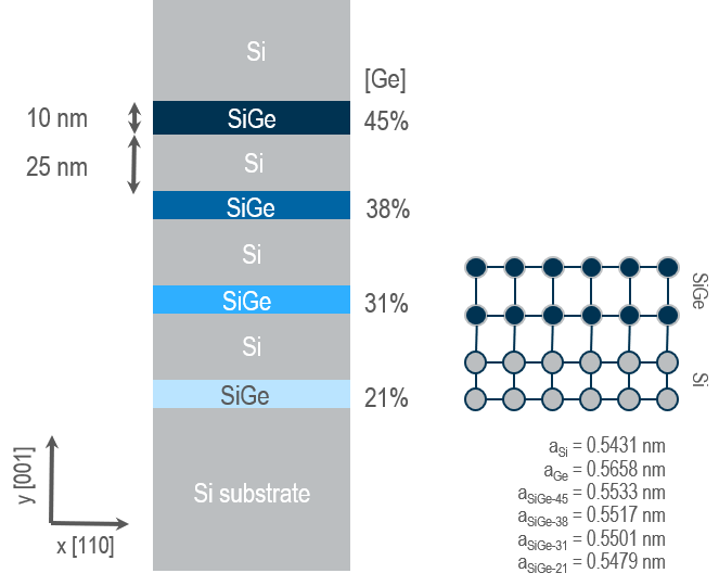
The sample data we use here was provided by the researchers at the Ernst Ruska Center for Microscopy and Spectroscopy with Electrons, Germany.
The sample is a Si/SiGe multilayer with four layers of SiGe with different Ge concentrations (21%, 31%, 38%, 45%). It was epitaxially grown without any dislocations. Since the lattice parameter of Ge (0.5658 nm) is larger than that of Si (0.5431 nm), we expect positive strain in the y (growth) direction and zero strain in the x (in-plane) direction. Based on simulations, strain in the y-direction is expected to increase with Ge concentration (up to 3% at the highest Ge concentration).
4D STEM diffraction data was collected with a STEM probe of ~3 nm and a semi-convergence angle of 0.6 mrad. Camera length was adjusted to make sure diffraction spots up to the 2nd order were captured with a sufficient signal-to-noise ratio in the diffraction image.
Strain calculation in DigitalMicrograph
Strain calculations in DigitalMicrograph are done on a 4D STEM diffraction data (NBED) using the Strain Mapping technique and palette (screenshot below) and following the flowchart above.
- Define the reference pattern.
The first step is to define a reference diffraction pattern from a sample region with no strain. In the above example, we use the Si substrate. DigitalMicrograph calculates an average diffraction pattern from all the pixel positions in the selected unstrained region (image N), then displays three red circles (center, u, and v unit vector selection) and one green circle (spots-spot search area selection) on this image.
Note: If you do not specify an unstrained area in the sample, the reference diffraction pattern will be generated using the full ROI. This means that the strain calculations will use an average (and not necessarily unstrained) reference and, as a result, not the absolute values.
In the reference pattern, specify a few parameters while keeping in mind the following considerations:
- Unit vector selection: The three red circles on the reference diffraction pattern specify the center and the unit vectors (u and v) and are used to create a template to detect the rest of the diffraction spots in the search area.
- The center circle is usually positioned on the direct beam (the center of the diffraction pattern). The size of this circle sets the area used to generate the diffraction disk template, so you should choose its size to be large enough to include a margin around the visible disk but not so large as to get close to any other disk.
- The u and v circles are positioned along the crystallographic directions for which the strain is to be calculated (e.g., in-plane and growth directions, respectively). The size of these circles defines the search radius used when analyzing all of the diffraction patterns to find the spot centers.
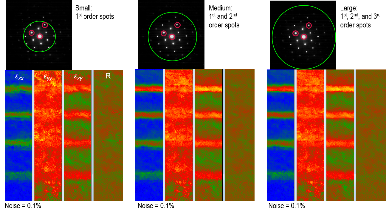
Note: As shown below, selecting the higher-order diffraction spots results in longer u and v unit vectors. This means the lower-order diffraction spots are excluded in the strain calculations, and the noise will be higher in the resulting strain maps.
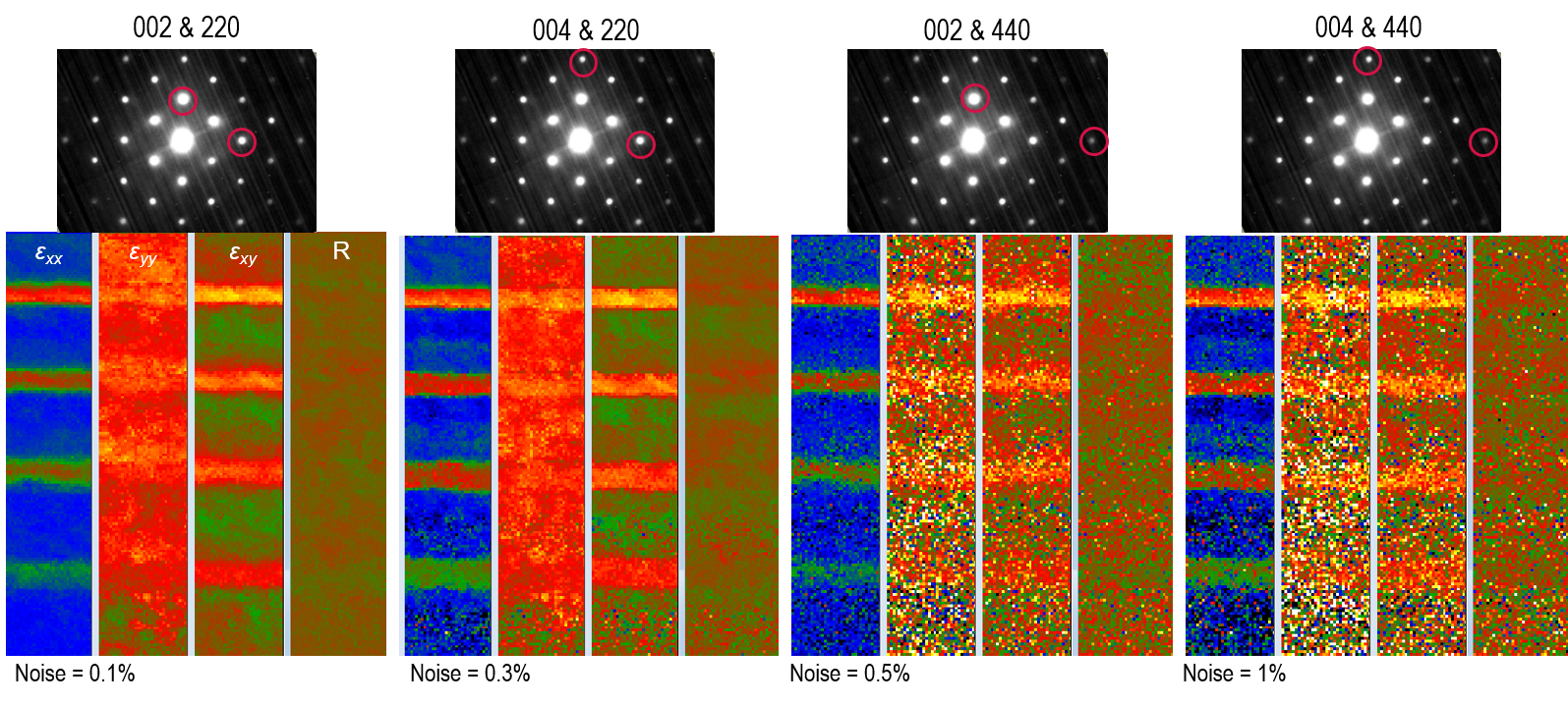
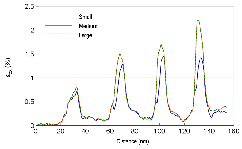
Spot search area selection: DigitalMicrograph only searches for diffraction spots in the area selected by the green spot circle. The smaller circle means a smaller search area per diffraction image, which speeds up the strain calculations. On the other hand, the diameter of this circle defines how many orders of the diffraction spots are used for these calculations. As shown below, although the noise is not much affected by this selection, including higher-order spots in the calculations results in strains closer to what is expected for this specimen from simulations (strain should increase with Ge concentration).
- Create a disk template.
The center spot marked on the reference diffraction pattern generates a template representing the shape of all the disks in the dataset. This template (image E in the screenshot above) is used along the directions of the u and v unit vectors to find the position of all the spots on diffraction patterns at each STEM probe position to calculate the strain.
- Calculate the strain maps.
Now that all the parameters are defined, strain maps can be calculated. DigitalMicrograph uses the u and v unit vectors and the disk template from the last two steps to calculate the best-fit lattice for each diffraction pattern (probe position). The strain is then calculated using the lattice deformation compared to the reference lattice (see the Background section). A couple of other points to consider:
- In the current implementation, DigitalMicrograph calculates the projected strains along the horizontal and vertical axis of the diffraction pattern and not the crystallographic directions specified by u and v vectors. The user is encouraged to measure the diffraction rotation angle during the microscope session and input this value to be applied to the diffraction patterns before strain calculations.
- During strain calculations, if the scattered intensity in diffraction spots for a specific probe position is small, then DigitalMicrograph does not perform any analysis on that diffraction pattern, and the strain components are all set to zero at that location.
As mentioned above, accurate determination of the position of the diffraction spots is critical for these measurements. Currently, DigitalMicrograph uses cross-correlation for this purpose. To better compare different correlation methods, please read Ultramicroscopy 176 (2017) 170–176.
Acknowledgments
J. Ciston and C. Ophus (National Center for Electron Microscopy, CA, United States) consulted on the development of the strain mapping technique in DigitalMicrograph. We would also like to thank T. Denneulin and V. Migunov (Ernst Ruska Center for Microscopy and Spectroscopy with Electrons, Germany) for providing this dataset, figures, and discussions on parameter optimization for strain calculations.