Automated in-situ spectrum imaging with synchronized stimulus control
Introduction
Spectrum imaging (SI) is a well-established technique allowing the collection of spatially resolved chemical or crystallographic information at high spatial resolution in the scanning transmission electron microscope (STEM). Combining electron energy-loss spectroscopy (EELS), energy dispersive spectroscopy (EDS), and convergent beam electron diffraction (CBED) capture into single multimodal SI acquisitions coupled with automated and synchronized in-situ stimulus, maximizes sample utilization for single-shot in-situ SI experiments.
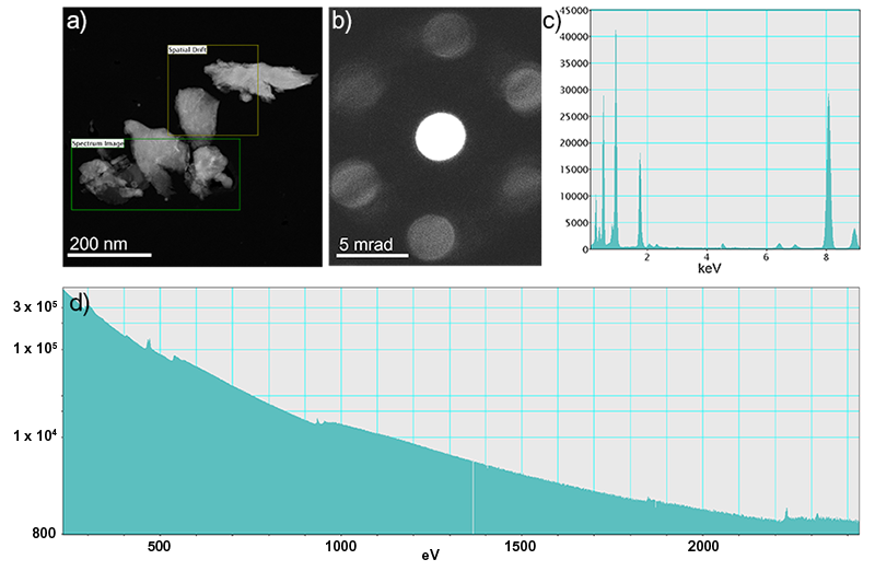
Transmission counting detectors provide a very sharp point spread function (PSF) and high sensitivity, allowing high signal-to-noise ratio data to be acquired at high resolution without sacrificing the field of view (FOV) [1]. These advantages can be leveraged in an energy filter for filtered imaging and EELS data acquisition. In the case of EELS, the sharp PSF enables a large number of ionization edges to be captured in a single spectrum while maintaining the energy resolution required for fine structural analysis (Figure 1, Figure 3).

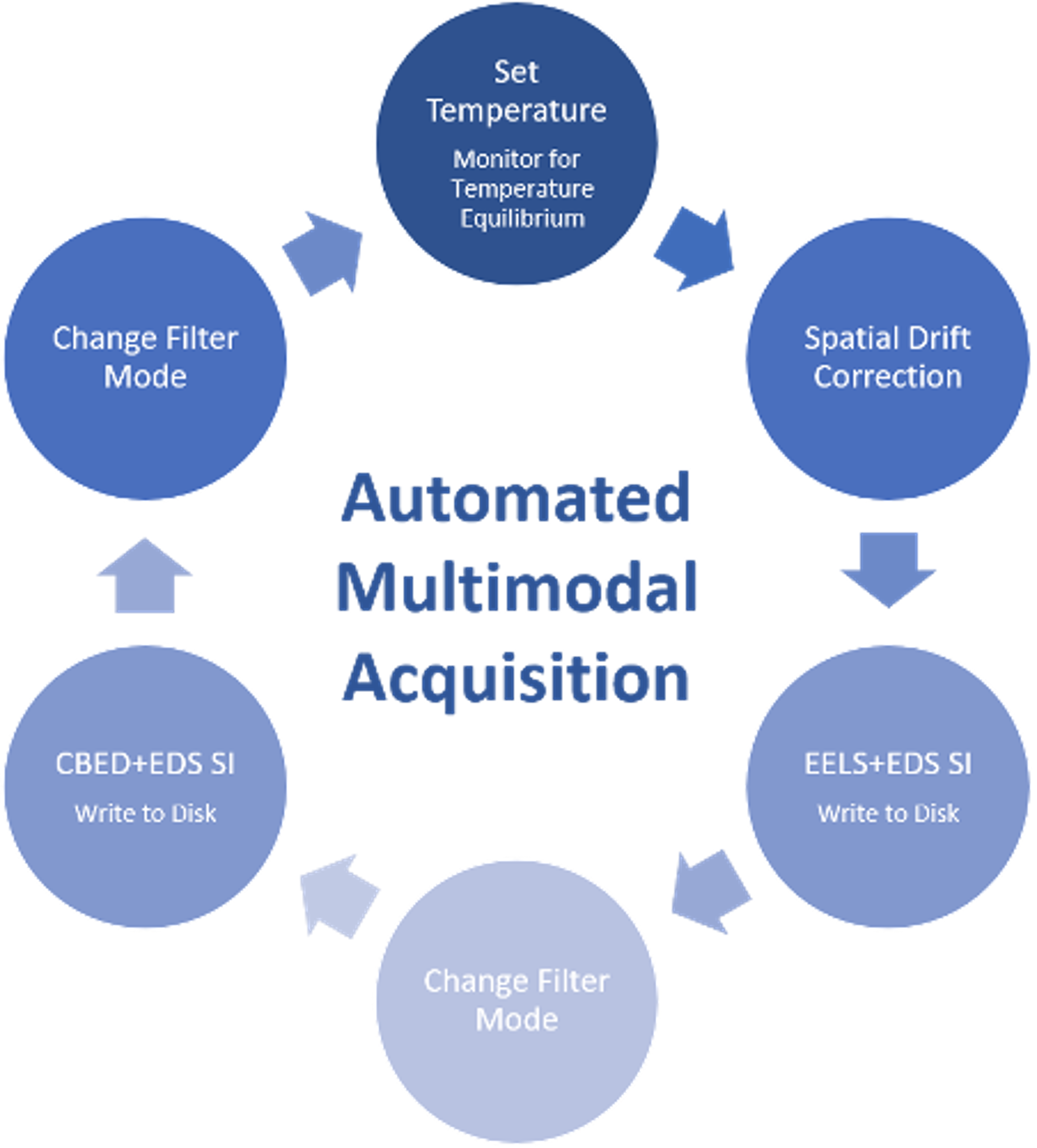
EELS and 4D STEM data cannot typically be acquired during the same experiment. Still, a customized workflow has been created using DigitalMicrograph® scripting, allowing fully automated acquisition of multiple pass (EELS, EDS, and energy-filtered (EF) CBED) spectrum images as shown in Figure 2. SI data was streamed directly to the disk during acquisition, enabling large amounts of data to be obtained at high in-situ stimulus resolution without being limited by system RAM.

Experiment
Copper (II) oxide powder was heated in 2 °C increments from 100 to 540 °C, in-situ, using a DENSsolutions Wildfire holder. EELS, EDS, and EF-CBED SI datasets were captured at each step using a GIF Continuum® K3® HR system and STEMx. EELS data was acquired at 0.9 eV/ch to maximize energy field of view (FOV) (~ 3 keV) and collection efficiency while also allowing single-channel spectral resolution to be achieved (e.g., 0.9 eV). This energy resolution allowed energy loss near edge structure (ELNES) (O K) and oxidation state (Cu L) mapping in addition to conventional elemental mapping, which was performed using both EELS and EDS data. CBED data was acquired with a 20 eV energy selecting slit centered at 0 eV. EF-CBED data was used to generate 4D STEM maximum spot maps (MSM) following the approach previously described by Miller et al. [2].
![Figure 3. CuO heating results from 100 to 540 ºC. Copper oxidation state and oxygen ELNES maps were produced using standards-based EELS quantification and concurrent standards as described by Schaffer et al. [3]. Counting EELS combined with EDS also allowed mapping of the: carbon K, nitrogen K, copper K, titanium L and K, iron L and K, and silicon K signals, as shown in the inset figures for selected temperatures. PCA denoised single scatter distribution of oxygen K and copper L spectra extracted from the annotated region are also shown. CuO heating results from 100 to 540 ºC. Copper oxidation state and oxygen ELNES maps were produced using standards-based EELS quantification and concurrent standards as described by Schaffer et al. [3]. Counting EELS combined with EDS also allowed mapping of the: carbon K, nitrogen K, copper K, titanium L and K, iron L and K, and silicon K signals, as shown in inset figures for selected temperatures. PCA denoised single scatter distribution oxygen K and copper L spectra extracted from the annotated region are also shown.](/sites/default/files/Figure3_3.png)
Conclusion
In-situ EELS, EDS, and 4D STEM spectrum imaging was performed at elevated temperatures in vacuum to measure changes in copper (II) oxide chemistry and crystallography with changing temperature. Maximum spot maps calculated from 4D STEM data show some change in grain orientation, but no clear trend was observed. A single channel FWHM of 0.9 eV/ch was found to be sufficient to perform EELS quantification on the copper L edge using a concurrent standards-based approach and identify a change in copper oxidation state from majority Cu(II) at 100 °C, to majority Cu(0) at 540 °C. Oxygen K edge fine structure mapping performed by the same method was in close agreement. Oxygen K maps using a copper (II) oxide oxygen standard showed high intensity in copper-rich regions of the sample at 100 °C, but this intensity was negligible at 540 °C. Zirconium, titanium, and iron-based impurities were identified in the target region of interest due to the large energy field of view provided by the GIF Continuum K3 at 0.9 eV/ch. EDS mapping was in good agreement with all EELS mapping performed. The automated acquisition methodology was shown to be an effective means of acquiring EF-CBED, EELS, and EDS datasets as part of a single-shot experiment. Such an approach could be widely applied to many other materials systems in the future.
References
[1] Hart, J. L., Lang, A. C., Leff, A. C., Longo, P., Trevor, C., Twesten, R. D., Taheri, M. L. (2017). Scientific reports, 7(1), 8243.
[2] Miller B., Pakzad A., Spillane L., Schaffer B., Czarnik C., (2021) EMAG – In-situ microscopy.
[3] Schaffer, B., Spillane L., Thomas P. J., (2019) Microsc. Microanal. 25 (Suppl 2).