Fast STEM spectrum imaging using simultaneous EELS and EDS in DigitalMicrograph software
Up to now, researchers performing analytical investigations in the transmission electron microscope typically had to choose between analytical spectroscopy techniques. They might choose energy dispersive x-ray spectroscopy (EDS) analysis when working with thick samples containing high-Z elements, or choose electron energy loss spectroscopy (EELS) when studying low-Z species in thin samples. With the advent of scanning transmission electron microscope (STEM) instruments with both high mechanical stability and high brightness probes, coupled with the latest generation of fast, efficient x-ray and EELS detectors, choosing among complementary techniques is a significant restriction. The acquisition systems available up to now have forced a choice because EELS, EDS, and fast scanning have not been designed to work together, resulting in inefficient data collection once the acquisition time per pixel dropped below a few tenths of a second.
In this paper, we present a data collection system that is designed to allow EELS, EDS and dark field detectors to operate efficiently at spectral rates over 1 kHz. This is achieved by allowing each detector system to acquire data independent of the other. The data collection systems are, however, linked together by a synchronization clock pulse to ensure the resulting datasets are in exact spatial alignment. The system described here has been recently implemented using DigitalMicrograph® software, also known as Gatan Microscopy Suite®, together with the Bruker Esprit EDS system. The necessary timing precision is achieved by hardware synchronizing the EELS and the EDS spectrometers with the beam scanning system as shown schematically in Figure 1. During simultaneous spectral acquisition, the EELS spectrometer provides system synchronization by means of a clock pulse at the end of each acquired frame. This pulse is used to advance the beam position and to inform the EDS system that the pixel has advanced. The EELS and EDS data is stored locally in software buffers and transferred asynchronously to the host application to ensure no data is lost. This mode of acquisition can be performed with any combination of the available signals and is also compatible with other features such as DualEELS™ acquisition and spatial drift correction.
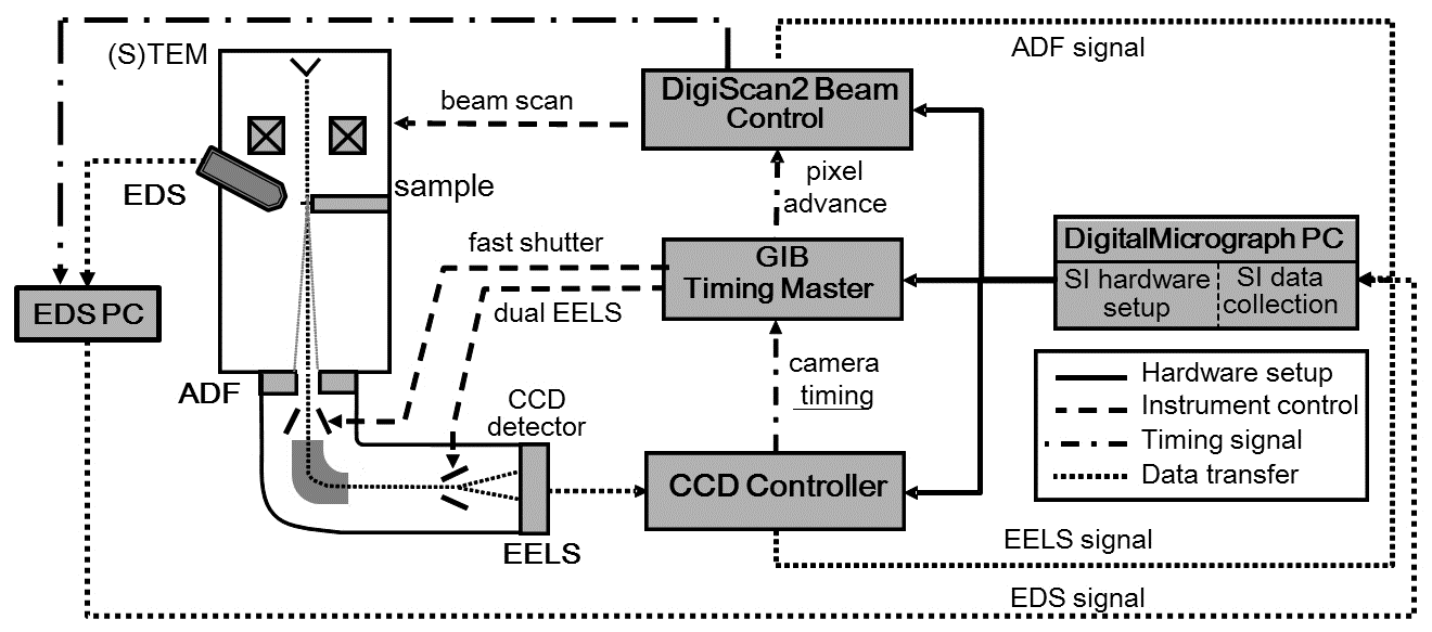
To illustrate these advances, data was acquired at TU-Graz in Austria using a probe corrected FEI Titan G3 STEM equipped with X-FEG high-brightness electron source operating at 300 kV. The instrument is also equipped with 4 quadrant SDD detector (FEI Super-X) controlled by the Bruker Esprit system and a GIF Quantum® ERS imaging filter for EELS acquisition. The EELS spectrometer is configured with the following features: (a) DualEELS capability that allows two different regions of the EELS spectrum to be recorded nearly simultaneously (Dt = 10 μs); (b) a low dispersion mode that allows EELS data to be recorded with an energy range up to 2000 eV (or 4000 eV in DualEELS mode); (c) a fast 2-k CCD that allows EELS acquisition at over 1000 spectra per second; and (d) dodecapole lens system capable of correcting spectral aberrations up to the 5th order allowing collections angles well over 100 mrad to be used while maintaining sub-eV energy resolution. The sample analyzed consisted of Pd/Au catalyst nanoparticles kindly provided by Professor Jianfang Wang’s group at the Chinese University of Hong Kong. The particles were deposited on a carbon film supported on a Cu mesh TEM grid. Data was acquired using a 220 pA STEM probe as indicated by the microscope fluorescence screen. The STEM is capable of much higher currents, but a relatively low current was needed to minimize sample motion cause by local heating. The probe convergence angle was 20 mrad and the collection angle was 35 mrad. Four different signals (annular dark field (ADF), EDS, EELS high core-loss and low core-loss) were recorded simultaneously. The EELS spectrum image (SI) was acquired in DualEELS mode; the regions of the EELS spectrum from 200 – 2200 eV and 1800 – 3800 eV were acquired using acquisition times of 7 ms and 30 ms, respectively. EDS spectra were acquired simultaneously, integrating counts over the entire pixel time employed for the EELS acquisition. This resulted is an EDS pixel time of 39 ms and nearly 100% live time. The count rate was approximately 15k counts/s in the center of a typical Au particle.
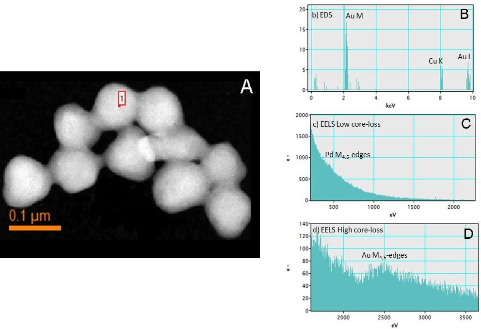
Figures 2B-D show EDS and high and low core-loss EELS spectra from a single pixel extracted from the region shown in Figure 2A. The EELS spectra show a good amount of signal; the Au M4,5-edges at 2206 eV stand out well above the background and a small amount of Pd is evident. The EDS data shows Au x-rays as well as Cu fluorescence.
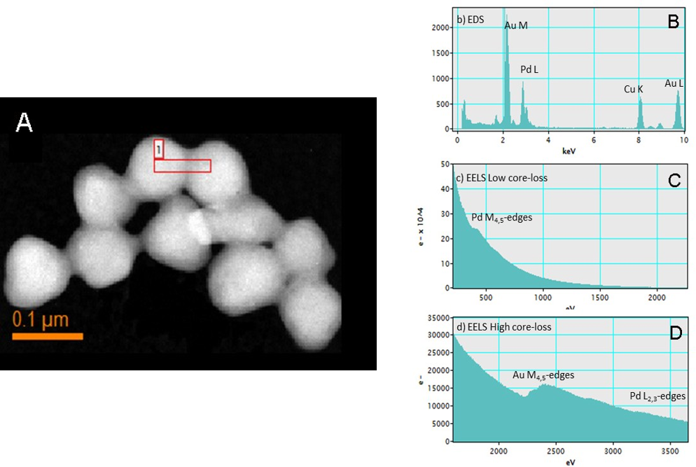
The quality of the spectra for both EELS and EDS dramatically improve after summing adjacent pixels together as shown in Figures 3B-D where 168 pixels across the region shown in Figure 3A were summed. In the summed EDS spectrum, the lines for all the elements present in the sample are observed and also in the Cu supporting grid as a result of poor localization of the EDS signal. The lack of a Cu L2,3 edge at 931 eV in the EELS data verifies the nature of the EDS artifact. The EELS low and high core-loss spectra appear to be virtually noiseless due to the very high counting statistics in the data. The Pd M4,5-edges at 335 eV appear to be very strong as well as the Au M4,5-edges at 2206 eV in the high core-loss spectrum. It is also interesting to note there is sufficient signal in the summed EELS data that the high energy Pd L2,3-edges at 3170 eV are also well above the background level and can be used for analysis if needed.
These results demonstrate that when the EELS system and STEM are properly configured, high energy edges can be recorded with high signal-to-noise ratio using short exposure times. This illustrates the suitability of EELS as a technique to analyze materials containing heavy metals such as Au.
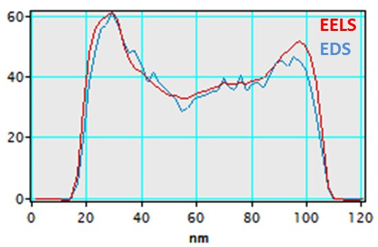
Figures 4A and 4B show the Pd elemental maps for EDS and EELS, respectively. In the case of EDS, the map was extracted using the La lines at 2.84 kV using an empirical Kramers background fitting followed by multiple linear least square (MLLS) fitting of each peak family represented by a set of Gaussian peaks. In the EELS case, the Pd M4,5-edges at 335 eV was used. The signal overlap with C K-edge of the underlying support film at 284 eV is easily separated using MLLS fitting. MLLS curve fitting of the overlap is only possible when the SNR for each individual pixel is sufficiently high as is the case in the EELS data. The EELS elemental map for the Pd looks much sharper and shows higher contrast than the same map obtained using EDS. This can be directly attributed to the strong forward scattering of the EELS signal and the nearly 100% collection efficiency of detector. The high SNR in the data is evident from intensity line profiles (5 pixel wide average) shown in Figure 5. The profiles are extracted from the region indicated in the red box in the EDS and EELS Pd elemental maps of Figure 4.

Figures 6A and 6B show the Au elemental maps obtained using EDS and EELS, respectively. In the case of EDS the elemental map was obtained using the Au Ma line at 2.12 kV using the fitting procedure as defined above. The EELS Au M4,5-edges at 2206 eV were extracted using power law background fitting. For Au, there is also higher quality in the EELS elemental map compared to that from EDS, despite the copious flux of x-rays from a heavy element such as Au. The Au elemental map obtained using EELS is sharper and shows more details than the same map using EDS.
To measure the relative quality of each map, the signal intensity was analyzed from a uniform region of an Au particle. This 16 x 16 pixel region is show by the red box in Figure 6 and the extracted data is summarized in Table 1. The SNR for the EELS data is ~17 while that for the EDS data is ~8 giving about a 2x improvement for the EELS data. However, for the EDS data, the SNR is largely limited by counting statistics (noise is approximately equal to the square root of the signal), while the EELS data is limited by the total signal (Au M edge + underlying background). This shows the clear difference between SNR and signal- (or peak-) to-background ratio (P/B). P/B determines what is possible to measure from a sufficiently long exposure while SNR determine what can be extracted from any given data set. For the data measured in this experiment, the EELS signal is more than twice as sensitive as the EDS data. Increasing either the collection efficiency or the dwell time for the EDS signal by a factor of 4 is required to match the EELS signal in this dataset.

| Mean signal (counts) | Standard deviation (counts) | SNR | |
| Au M EELS Map | 14,468 | 856 | 17:1 |
| Au M EDS Map | 79.9 | 10.1 | 7.9:1 |
Figures 7A and 7B show colorized elemental maps of Pd and Au obtained using EDS and EELS respectively. Qualitatively, the EELS maps appear to be sharper and show much higher contrast. In particular, significant details are absent in the EDS maps which are clear in the EELS maps. For example, the diffusion of the Pd into the Au region is difficult to discern in the EDS maps whereas this appears to be clear in the EELS maps.
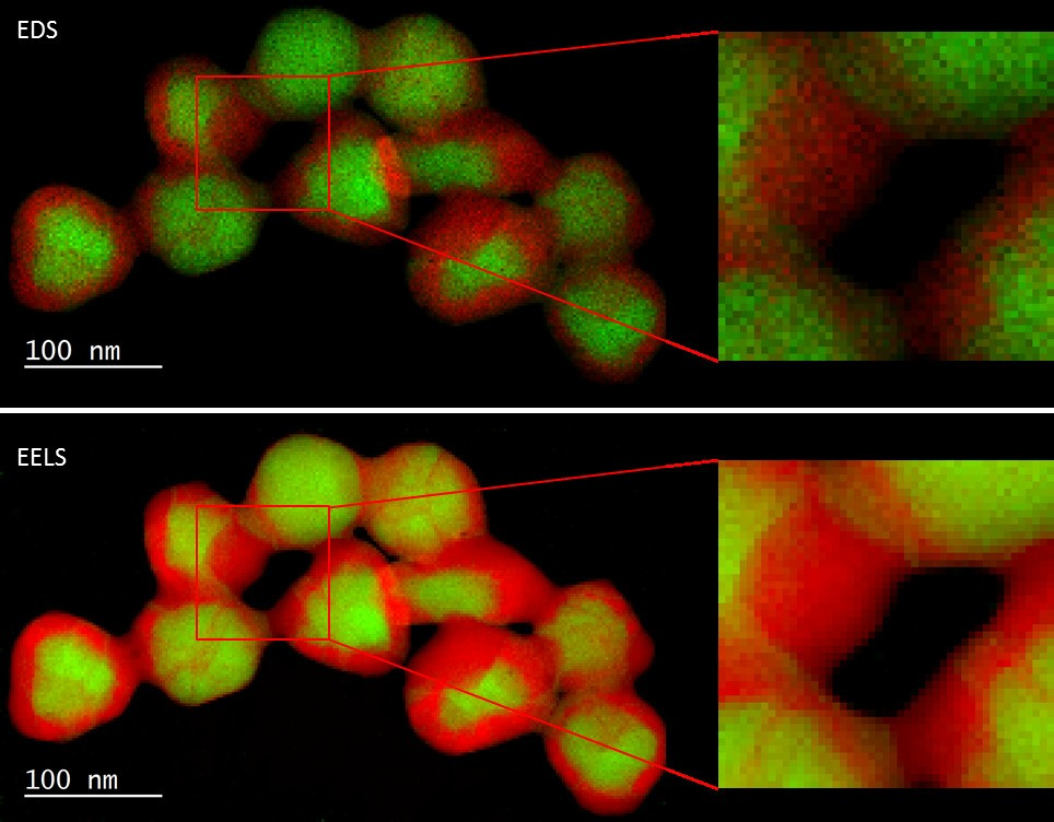
The EELS and EDS data presented here can be regarded as highly complementary. The main difference is that for the EDS case, each pixel carries little information due to the very low SNR of the data even at these long exposure times and with high fluorescence yield materials. However, the high signal-to-background ratio (SBR) of the EDS technique allows summation of adjacent data almost indefinitely improving the detection limits at the expense of spatial resolution. The EELS data, on the other hand, has very high collection efficiently resulting in high SNRs for each pixel acquired. Summing adjacent pixels improves the detection limits considerably but will show diminishing returns once the shot noise in the signal integral becomes irrelevant. The techniques further complement each other when identifying artifacts in the data. For example, secondary fluorescence and preferential absorption in the EDS data can determined from the EELS data, while possible missing elements in the EELS data range acquired can be identified in the summed EDS signal.
Having a system for fast and efficient acquisition of both EELS and EDS spectra allows the routine collection of both of these complementary data signals. There is no longer a need to choose between analytical techniques; both EELS and EDS can be acquired easily with every data run. The data presented here shows the complementary nature of having both high SNR and high SBR data acquired at the same location, at the same time. Further, the ability of combining composition measurements from EELS and EDS with physical and electronic information also available only from EELS (e.g., plasmonic, band gap and density of states information) promises to open whole new avenues of materials analysis.