eaSI™: STEM experiments combined, synced, and linked.
WHAT IS STEM SPECTRUM IMAGING?
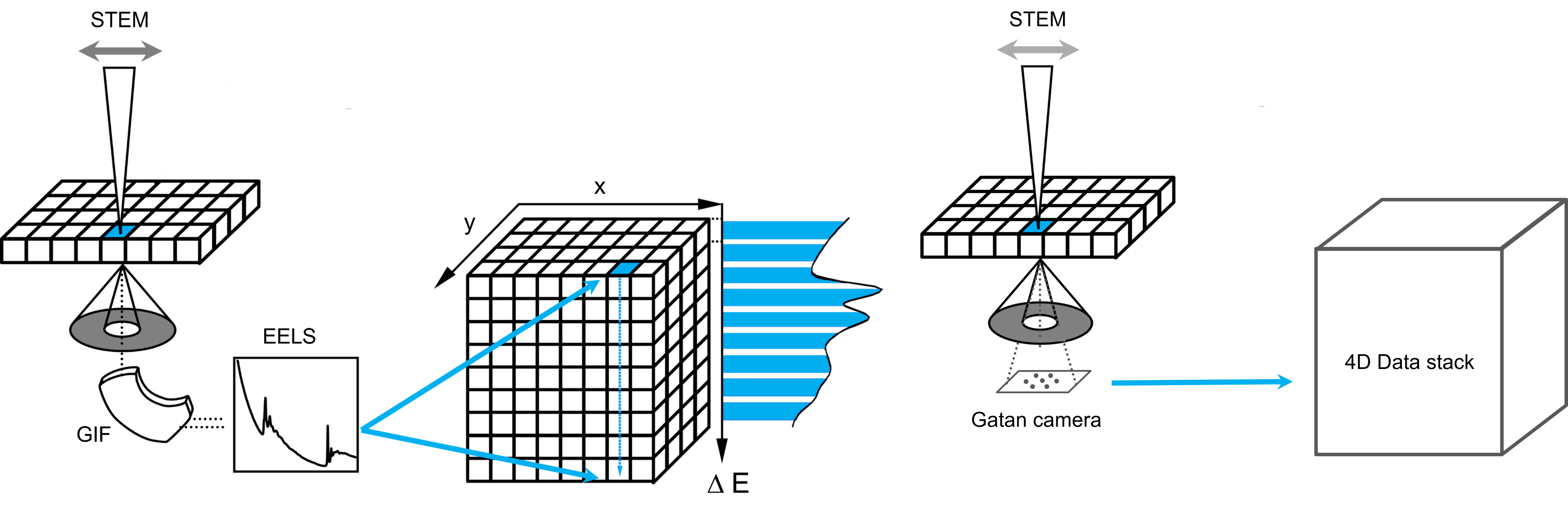
In scanning transmission electron microscopy (STEM), the electron beam is focused on a fine spot, varying from a few nanometers down to nearly atomic dimensions, on an electron-transparent specimen. As electrons interact with the specimen and scatter, diverse analytical signals are produced: 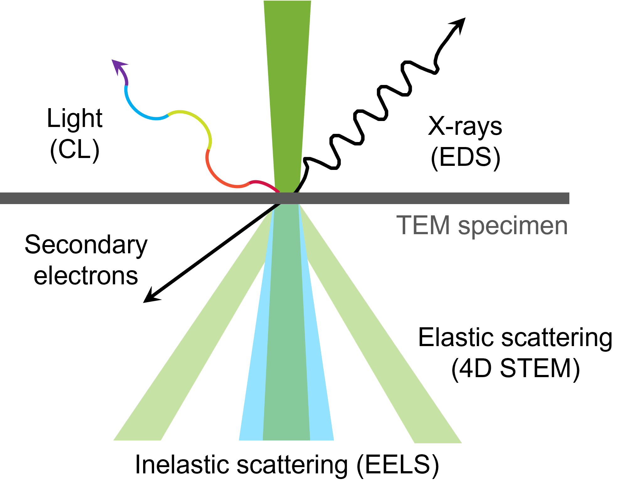 As electrons interact with the specimen and then scatter, generating different types of analytical signals:
- X-rays (EDS)
- Light (Cathodoluminescence)
- Secondary electrons (DigiScan 3)
- In-elastically scattered electrons (EELS)
- Elastically scattered electrons (4D STEM)
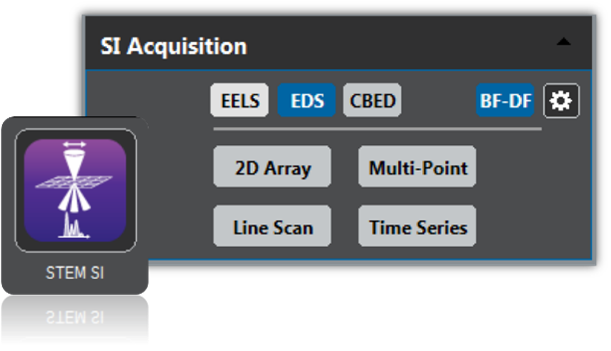 You can then record a spatially resolved distribution of one-dimensional (1D) spectra or two-dimensional (2D) diffraction images in scanning mode to build 2D, 3D, or 4D datasets that unveil remarkable details in the specimen. This technique, known as spectrum imaging (SI), systematically probes a defined specimen area (multiple points, line scan, or a 2D array) to automatically collect the maximum possible information.
WHAT IS eaSI
Analyzing a specimen with a single STEM technique is often insufficient to fully understand the system and explain/predict the material properties/behavior. As a result, in most STEM experiments, multiple complementary signals from various detectors can be recorded (STEM imaging, EELS, EDS, and 4D STEM). In this case, the challenge is ensuring that data streams collected on different detectors are spatially and temporally correlated and analysis workflows for such correlated data are not complex. eaSI makes this possible.
|
Combine: Spatial correlation between data streams |
 |
|
Sync: Temporal correlation between data streams |
 |
|
Link: Common tools for analysis of correlated data |
 |
EXAMPLES of eaSI
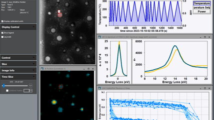
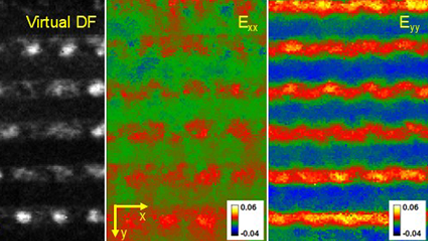
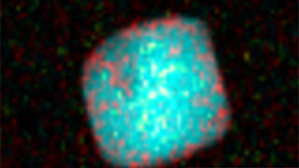
In this dataset, a fully automated multimodal in-situ heating experiment captures the reduction of copper oxide to metallic copper. This irreversible thermal decomposition involves simultaneous microstructural, crystallographic, and chemical changes. This experiment is challenging in conventional systems since it requires multiple analytical techniques (EELS, EDS, and 4D STEM). Recording spatial and temporal evolutions within a sample often requires heroic manual effort.
eaSI uses a single computer and software interface throughout this experiment to automatically combine (spatially) and synchronize (temporally) signals from different detectors. Compared to a manual experiment, eaSI automation improves temperature resolution by 25x, TEM-user productivity by 300x, and eliminates unavoidable inaccuracies associated with human error.

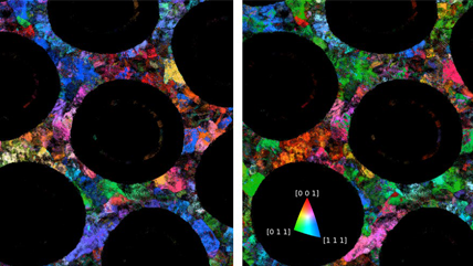
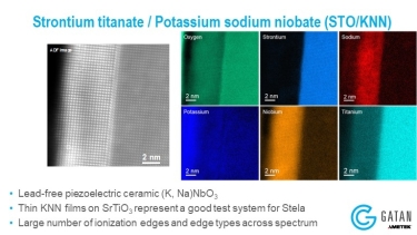
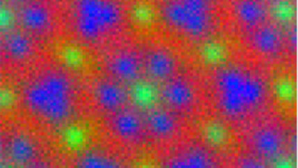
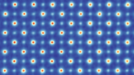
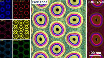
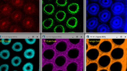
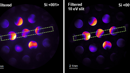
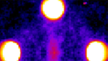
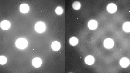
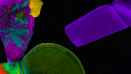
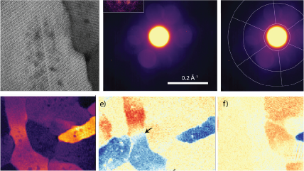
Once a multimodal dataset collection is complete, it must be analyzed and processed. The below results demonstrate how eaSI enables users to examine true spatially correlated chemical (EELS) and crystallography (4D STEM) data collected as a part of a single STEM experiment within DigitalMicrograph software. eaSI links STEM datasets and provides common tools for analysis of the correlated EELS and 4D STEM data. Here, 4D STEM virtual aperture analysis was first performed to identify distinct crystallites in gadolinium-treated carbon nanohorns. Then, EELS spectra from the exact same crystallites were analyzed to confirm that both gadolinium and oxygen were present in these areas.
ADVANTAGES OF eaSI
| Capability | Advantage |
|---|---|
| Right tools for multimodal STEM studies | Encompasses the broadest range of STEM-optimized EELS, EDS, and 4D STEM detectors to propel your studies forward |
| It brings a new dimension to your research | Allows you to observe dynamics in-situ within your 3D EELS, EDS, and 4D STEM datasets so you can better understand nanomaterials and devices in real time and under real-world conditions |
| Seamlessly links multimodal and dimensional data | Links 3D, 4D, and even 5D SI data within DigitalMicrograph so you can visualize novel chemical–, compositional–, morphological–, and structure-function information in your materials and devices with a greater degree of confidence |
| Shortens the time to meaningful results (set up, acquisition, and processing) | Regardless of your level of expertise, utilize the most efficient workflows within a single DigitalMicrograph interface to deliver multidimensional and correlative results within minutes. |
| Ensures no compromise between speed and functionality | Leverages the leading DigitalMicrograph STEM SI technique to coordinate complex transitions and eliminate downtime between modes while maintaining the high precision you expect in a standalone experiment |
| It makes the impossible possible | Utilizes scripting to easily expand workflows to address more complex studies and diminish the need for hero experiments |


A powerful tool that expands the utility of your Gatan camera to address 4D STEM diffraction studies.

Electron counting for all your EELS, EFTEM, and energy-filtered 4D STEM applications.

The most intuitive and easy-to-use energy dispersive spectroscopy (EDS) tool for scanning transmission electron microscope (STEM) applications and in-situ microscopy.

A powerful method of obtaining detailed analytic data from a sample on an electron microscope equipped with scanning mode.

DigitalMicrograph, also known as Gatan Microscopy Suite, drives your digital cameras and surrounding components to support key applications including tomography, in-situ, spectrum and diffraction imaging, plus more.

Digital beam control and image processing to enhance the photographic quality of your digital images.


Quantify microstructural changes in materials due to applied mechanical loading.

Diffraction analysis package (DIFPack) to automate the selection area of your electron diffraction (SAED) patterns and high resolution lattice images of crystalline samples.

Simulation tool to eliminate the guesswork from your EELS and EFTEM compositional mapping experiments.

High-angle annular dark field (HAADF), annular dark field (ADF) plus bright and dark field (BF/DF) detectors for STEM imaging optimized for electron energy loss spectroscopy (EELS).


The EELS and EFTEM systems ideal for multiuser facilities, now with the Stela hybrid-pixel option.

Enabling optically-coupled transmission electron microscopy to reveal nanoscale structural, optical, and electronic properties


")


Applications
eaSI 4D STEM Applications
eaSI EELS Applications
![360 x 50-pixel 2D array dose fractionated EELS SI acquired from SRO/[110] DSO with a 339 µs pixel dwell time.](/sites/default/files/images/2D_Array_Dose_Fractionated_EELS.jpg)
Posters
|
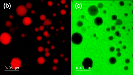
Continuous EELS spectrum imaging of nano-droplet crystallization heterogeneity - EMC 2024 |
Using open-source Python packages in DigitalMicrograph for analyzing 4D STEM - IMC 2023 |
|