Examples of In Situ Advantages of In Situ
WHAT IS IN SITU?
In-situ transmission electron microscopy (TEM) combines the image formation capabilities of the TEM with the applications of one or more external stimuli to observe real-time sample dynamics. A diverse array of systems and holders allow researchers to apply various stimuli, unlocking the potential to evaluate dynamics during electrical biasing, mechanical strain and deformation, heating, cooling, light illumination, and the introduction of gaseous or liquid environments, as well as intense electron beam irradiation.
Historically, movies of various reactions and system kinetics were recorded on videotape. With the advent of screen capture programs, this process improved, allowing low-resolution, qualitative video capture to visualize what is happening at speeds up to video frame rates, e.g., 30 frames per second (fps).
With advancements in data transfer and processing capabilities, Gatan in-situ cameras can now record and manage large datasets directly from the sensor output. The original quantitative data from each frame captured during an experimental session can be stored directly on disk and treated as individual images or played back as a video.
Additionally, various algorithms or scripts (e.g., summing, drift correction, and binning) can be applied after capture to extract the most useful parts of the acquired data. The free built-in data management tools available for Gatan in-situ cameras allow data to be isolated and extracted easily so that post-processing data analysis can be performed to quantify the observed effects of the stimuli applied to the system.
This streamlined data capture and post-processing workflow significantly increases the probability of acquiring publishable data during a microscopy session. The most advanced in-situ cameras from Gatan offer unprecedented resolution in both time and space, with sub-ms time resolution. This capability allows researchers to study reactions that were previously too fast to capture and resolve previously unknown dynamics.
Today, in-situ electron microscopy encompasses much more than just TEM imaging. Techniques such as scanning transmission electron microscopy (STEM) imaging, diffraction, electron energy loss spectroscopy (EELS), energy-dispersive x-ray spectroscopy (EDS), and 4D STEM can all be acquired continuously while varying stimuli. This allows for deeper insights into the dynamics of the structure, composition, and bonding of materials. Gatan provides the scientific community with tools to apply these techniques to in-situ experiments. Simple in-situ data collection is supported by automatic data synchronization and powerful tools for processing, analysis, and visualization.
EXAMPLES OF IN SITU
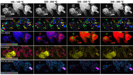
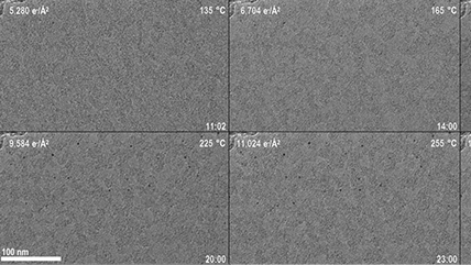
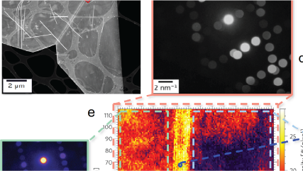
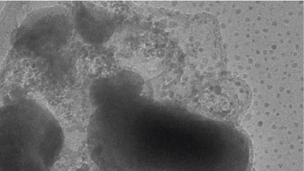
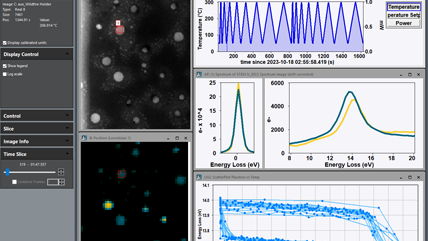
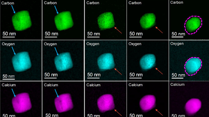
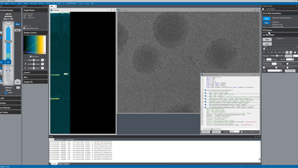
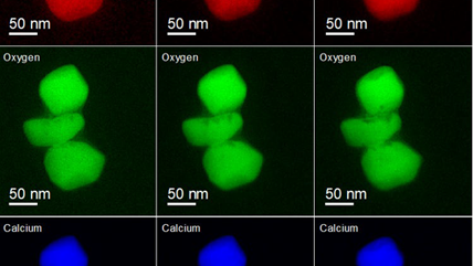
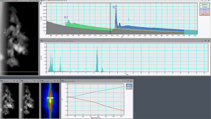
The in-situ upgrade to the GIF Continuum® makes in-situ EELS spectrum imaging with real-time quantification of oxidation state, real-time drift correction, and simultaneous EDS and ADF imaging possible. Here, 428 spectrum images were acquired at a rate of 1 every 5 seconds, or about 1 every 2 °C, as the FeOOH sample was heated to 850 °C.
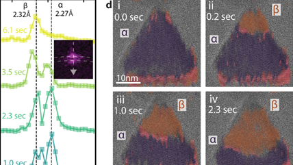
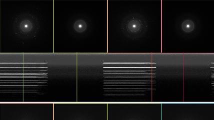
In-situ diffraction video datasets were captured using a Metro® counting camera without any beam stop as the temperature of VO2 oscillated above and below its metal-insulator transition temperature. This video shows the automatically synchronized playback of the original data, the same data after averaging every 10 frames, and the temperature. A linked profile tool is used to visualize better the line of diffraction spots, which only appear at low temperature when the VO2 is insulating.
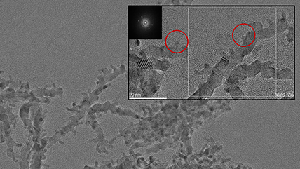
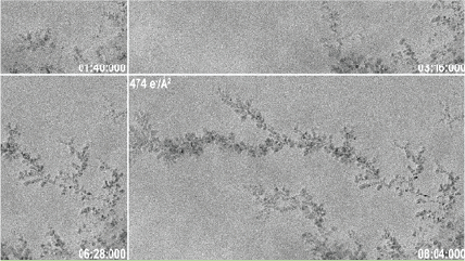
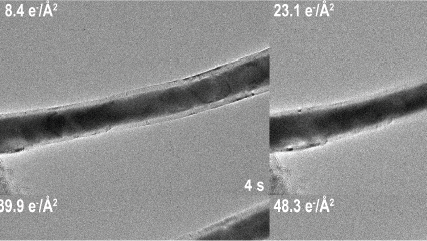
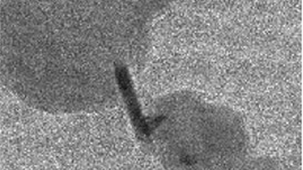
Low-dose TEM imaging enabled the observation of this beam-induced dendritic growth of Cu. A dose rate of just 1 e-/Å2/s resulted in a growth rate of approximately 10 nm/s. Observation of a 5.7 x 4.1 µm field of view with 0.5 nm pixels was made possible by the K3® IS camera, which captured 11520 x 8184 pixels at 5 fps.
ADVANTAGES OF IN SITU
| Capability | Advantage |
| Real-time observation | Rapidly collects data from a single sample to understand how materials change. |
| Environment and stimulus control | Captures how different environments and various stimuli can change the structure, properties, and performance of materials. |
| High spatial and temporal resolution | In-situ TEM can enable spatial resolutions from 10s of nanometers to fractions of an angstrom, plus temporal resolutions from a few seconds to less than a millisecond. |
| Operando investigation | Offers even greater insight when the material's performance and structure are measured during the application of different stimuli. |
| Variety of techniques | Electron microscopy encompasses more than just TEM imaging. It also includes STEM imaging, diffraction, EELS, EDS, and 4D STEM. These techniques can all be acquired continuously while changing stimuli, allowing for a deeper understanding of the dynamics related to the structure, composition, and bonding of materials. |

The cutting-edge counting camera for groundbreaking imaging, diffraction, and in-situ studies.

DigitalMicrograph, also known as Gatan Microscopy Suite, drives your digital cameras and surrounding components to support key applications including tomography, in-situ, spectrum and diffraction imaging, plus more.


Preserve sample integrity with controlled transfer from an inert environment to the TEM.


A powerful tool that expands the utility of your Gatan camera to address 4D STEM diffraction studies.

Single and double tilt heating holders for direct observation of microstructural phase changes, nucleation, growth, and dissolution processes.

Electron counting for all your EELS, EFTEM, and energy-filtered 4D STEM applications.

Facilitate your HREM assays by automatically adjusting the critical imaging parameters of a TEM microscope focus, stigmation, and beam tilt.

Latest CMOS camera that with its resolution, speed, and ease of use will revolutionize electron microscopy.

Quantify microstructural changes in materials due to applied mechanical loading.

Diffraction analysis package (DIFPack) to automate the selection area of your electron diffraction (SAED) patterns and high resolution lattice images of crystalline samples.

Designed to produce consistent, high-quality surfaces across semiconductors, batteries, and advanced materials using a single, integrated workflow.


The EELS and EFTEM systems ideal for multiuser facilities, now with the Stela hybrid-pixel option.

The high-performance scintillator camera that elevates your everyday transmission electron microscopy.


Applications